Quote of the Day
With hard work, difficult material can be grasped. Step by step, incrementally, the novice can become the master.
— Joshua Waitzkin. World Tai Chi champion and subject of the book 'Searching for Bobby Fischer'. He is working with Khan Academy to promote learning through hard work.
Introduction
I have never used a 555 timer for a home project and now I have several applications for this handy device up at my cabin in Northern Minnesota. I thought I would cover some of the basics in this post. Sure this material is covered in other places, but I need to work all the details myself to really understand a part. I like to document my learning here so that others can share in it -- and help me find any errors in my work.
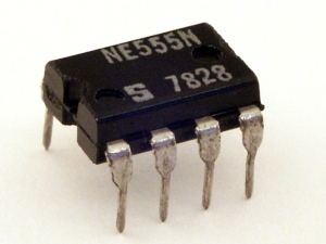
I first encountered the 555 when I was at university back in the 1970s. Eng Hoyme, the father of a very good friend, had designed a very impressive electronic organ using a bank of 555 timers. Figure 1 shows the NE555 in a DIP option − this is how I first saw it. It was always interesting for me to go into his basement and see all the stuff he was building. His oldest son had an old Altair 8800 system down their as well. This was my first contact with microcontrollers. It was exposure to their passion for electronics that helped light a fire in me for electronics − a passion that is even bigger today.
Background
Scope
There are an enormous range of applications for this part. My post here will cover the use of the 555 timer in a basic astable multivibrator configuration. My cabin application requires a low-frequency oscillator (27 kHz) that does not need to be very stable. The 555 is ideally suited for this type of application.
My objective for this blog post is to:
- Derive an expression for the frequency of a 555 timer when used as an astable oscillator.
- Derive an expression for the duty cycle of the 555 timer output when running as an astable oscillator.
- Create a Mathcad routine for finding component values that simultaneously meet my requirements for duty cycle and frequency.
Some Definitions
Let's define a few of the terms that I will be using.
- Duty Cycle (DC)
- Duty cycle is the percentage of one period in which a signal is active. In my case, active means that VOut = ~VCC.
- Time Constant (τ)
- A time constant is the parameter characterizing the response to a step input of a first-order, linear time-invariant (LTI) system. Physically, the constant represents the time it takes the system's step response to reach
of its final (asymptotic) value. For an RC system like this,
.
- Threshold Voltage (VThresh)
- As I use the term here, threshold voltage is the voltage at which a comparator will switch.
Block Diagram
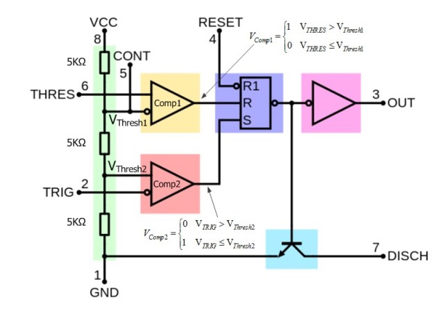
Figure 1 shows a block diagram of the 555 that I pulled from the Wikipedia and modified slightly.
We can glean numerous bits of information from Figure 2. I will highlight a few:
- The comparators are biased using 3, 5KΩ resistors.
I have heard it said that these three 5 KΩ resistors are the source of the name "555".
- The CONT pin gives you direct control of the upper comparator's threshold.
You cannot independently control the lower comparator's threshold, but you can use a resistor divider on the THRESH pin to give you similar control.
- The inputs of the two comparators are configured differently.
The upper comparator is configured to reset the internal flip-flop when the THRESH pin exceeds the high-level threshold. The lower comparator is configured to set the internal flip-flop when the TRIG pin is less than the high-level threshold.
It is amazing how flexible this simple architecture has proven. I have seen hundreds of different applications for this simple part.
Basic Astable Operation
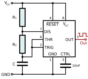
Figure 3 shows a 555 timer hooked-up in the standard astable configuration (Source).
The frequency of the OUT signal is set by the charge and discharge time of the RC circuit setup by R1, R2, and C. Charging of C is done by R1 and R2. Discharging of C is done by the DIS (DISCH in Figure 2) pin using R2 alone. Discharge time is only affected by R2 because the DIS pin will go to 0 V during the discharge cycle. This isolates R1 from the rest of the circuit.
The circuit of Figure 3 will always have a duty cycle greater than 50%. You can understand this by observing that OUT = "1" (high voltage) when R1 and R2 are charging C from the low threshold level to the high threshold level. OUT = "0" (low voltage) when C is being discharged from the high threshold to the low threshold through R2. The charge time constant is always longer than the discharge time constant, so the "1" time is always longer than the "0" time. This is equivalent to saying the duty cycle is always greater than 50%. I include a more formal derivation here.
There is an alternative circuit that will give you a 50% duty cycle output. Observe that this circuit uses the OUT pin to discharge C rather than the DIS pin. Thus, the same resistor value is used for both charging and discharging. The disadvantage of this circuit is that the output current drive must be shared between the timing circuit and the external load. This is not a good thing for some applications because the external load may change the circuit's oscillation frequency significantly.
Basic RC Circuit Modeling
The voltage across a capacitor in an RC circuit can be modeled using Equation 1.
| Eq. 1 |
where
- vC(t) is the voltage across the capacitor versus time.
- VInitial is the voltage across the capacitor at t = 0.
- VFinal is the voltage across the capacitor at t = ∞.
- R is the resistance of the resistor that is charging the capacitor.
- C is the capacitance of the capacitor being charged.
For a derivation, see this book.
Analysis
Oscillation Frequency
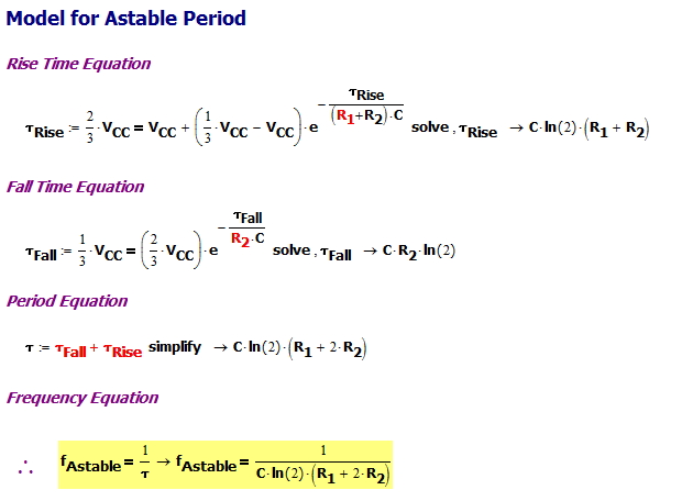
You can determine the oscillation frequency by applying Equation 1 to determine the rise and fall times of the voltage on capacitor C in Figure 3. Figure 4 shows my calculations.
Duty Cycle
My particular application requires that the 555 output have a specific duty cycle. We can compute the duty cycle from the circuit of Figure 3 using the formula shown in Figure 5.
Resistor Values in Terms of Frequency, Duty Cycle, and Capacitor Value.
I can use the formulas developed in Figures 4 and 5 to compute values for R1 and R2 in terms of the oscillator frequency, duty cycle, and the capacitance value. The derivation is shown in Figure 6.
For those requiring more details, I provide another example and a spreadsheet implementation of these formulas in the comments section of this post.
Check Against Simulation
To verify my equations, I simulated my example circuit using LTSpice. Figure 7 shows the circuit I simulated.
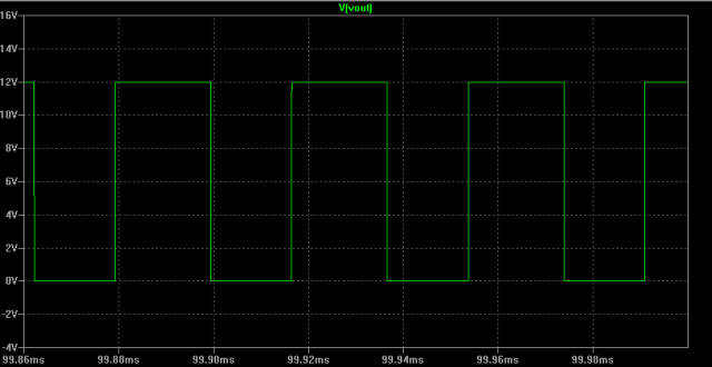
Figure 8 shows the output waveform from the circuit in Figure 7.
Figure 9 shows the error analysis of my measured values from my theoretical predictions.
I consider these errors pretty typical considering the modeling assumptions.
Conclusion
I would say that the majority of 555 circuits use some form of the astable configuration. It was a useful exercise for me to develop equations that will allow me to compute the required resistor values for a given oscillation frequency, capacitance value, and duty cycle.
Appendix A
Figure 10 shows a 555 astable circuit with 50% duty cycle (source -- a first-rate web page on the 555).
As I mentioned above, I cannot see using this circuit often because I prefer to keep my load circuit separate from my timing circuit. This makes the circuit's frequency more predictable.





How do you figure out C if you don't know R1 and R2? Based on equations, not physical parts.
Hi Daniel,
We have 3 components to determine: R1, R2, and C. In the model I show here, we have two performance parameters: frequency (f), and duty cycle (DC). I won't go through the theory here, but this means that one parameter is arbitrary, i.e we can make it any convenient value. Since resistors are available in far more values than capacitors, let's assume that we will select a capacitor value because fewer options are available. This means that we can compute the resistor values using the calculations shown in the following figure.
Because looking at Mathcad screenshots can be confusing, I included an Excel implementation here.
I hope this makes things clearer. You will find that many circuits will require that one component value be selected arbitrarily, and the other values are then determined in terms of that selection.
mark
the math applied changes when Diodes are placed to make a PWM output
I was simulating a 555 in astable mode to generate PWM, but with variable cycle duty, the circuit uses two fast diodes.
http://chemelec.com/Projects/PWM/PWM-1.png
But the equations does not match, so I replaced the diodes with schottky, and I realized that the frequency changed, so frequency also depends on the forward voltage of diodes. Could you make an approach to the new equations, since I haven't found yet. I'll try to do it myself. Thanks for your posts they're very helpful and awesome.
Take a look at this post. I hope it helps.
mark
Thanks for the post, it really helps!
If you have more questions, just ask. Because I am building a house and workshop right now, I may not answer immediately.
mark
In Figure 4, I'm not sure how you get the period "t" from the rise time (t_rise) and fall time (t_fall) of the natural response of the circuit described in Eqn. 1? The confusion comes from how we are defining the rise time and fall time? Are we defining them as the 10% - 90% rising edge of the pulse for the t_rise and the 90% - 10% falling edge of the pulse for the t_fall? Or are we defining t_rise as the time the pulse is high per period, and t_fall as the time the pulse is low per period?