Quote of the Day
We are what we repeatedly do. Excellence, then, is not an act, but a habit.
- Aristotle
Introduction
I often build small electronics projects for use around my home. I recently put together a small sensor interface that generates an output sine wave with a frequency proportional to the sensor's inductance. At my receiver, I want to convert that frequency to a voltage that is proportional to the sensor's inductance. I want to send out a text message when the value of the sensor's inductance passes through a threshold level – I am detecting the presence of a car (Figure 1).
Since this is a home project, I want to keep it simple and cheap. This blog post documents how I designed this circuit.
Background
The circuit I used is very slight variation on a charge pump circuit I saw years ago in the great little book called "Electronic Designer's Handbook" by Thomas Hemingway (Figure 13.5). This little gem can be viewed online here. The only change I made to this circuit was to shift the voltage levels so that my input signal can be positive.
I will derive an expression for the input frequency-to-output voltage transfer function that is a bit more accurate than what Hemingway derives. However, this is his circuit and his book is still worth reading for those interested in transistor-level design. As you can see, this book was first published in 1966 and I still use it nearly fifty years later.
Analysis
I will focus on my simulation results in this blog post section. Appendix A contains measured data from a working circuit in the field.
Schematic
Figure 2 shows an LTSpice schematic of the circuit I put together.
Theory of Operation
Qualitative Description
The circuit operation is fairly straightforward.
- When the input signal goes low, C1 charges through D1. It is critical that C1 charge quickly relative to the period. This circuit depends on the transfer a fixed quantity of charge at the same rate as the input signal. This means that the charge transfer rate (i.e. current) is directly proportional to the input frequency.
- When the input signal goes high, C1 discharges through Q1 into C2. C2 will have enough capacitance to ensure that it changes little when C1 discharges into it. This will provide the filtering we need to for a smooth output voltage.
- The RC filter composed of R1 and C2. R is critical in determining the gain (i.e. slope) of the output voltage versus frequency curve. At equilibrium, the charge lost through R1 for each input cycle exactly equals the charge on C1.
I included my simulation results below that clearly shows each of these operations occurring.
If you seek a more detailed narrative description of how this circuit work, see the discussion comments below. A reader put together an excellent theory of operation on the circuit.
Mathematical Details
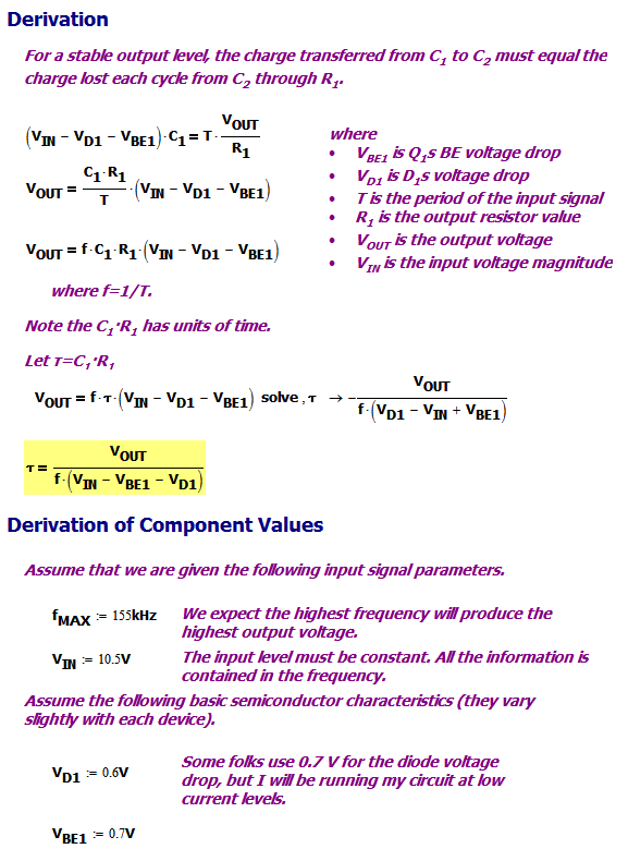
Figure 3 shows my derivation of a formula for the frequency-to-voltage conversion process.
Simulation Results
Single Simulation Result
Figure 4 shows my simulation results. To see these results clearly, you need to click on the image. The circuit operates exactly as described above.
Linearity Measurements
Figure 5 shows the linearity that I measured on the simulator. I predicted the slope of my voltage conversion to be 1.08 in Figure 2. My simulation shows 1.095, which means an error of ~1.4%. Not too bad.
Conclusion
This circuit is a critical part of a small home sensor system that I have put together. Here is a quick description of my sensor system.
- I built a metal sensor that is composed of a coil of wire (i.e. inductor) whose inductance decreases when a metal object comes near -- the inductance decreases because of how currents are induced in the metal object. This complex electrical process involved the use of specialist electronic tools such as wire strippers (wirestriper).
- I built an oscillator which puts out a digital signal with a frequency that is proportional to the inductance of my wire coil.
- The circuit described here converts the digital signal's frequency to a voltage level.
- I use a Schmitt trigger to generate an alarm when the voltage from my frequency-to-voltage converter exceeds a value that I have set.
Appendix A: Some Empirical Data from a Circuit I Built
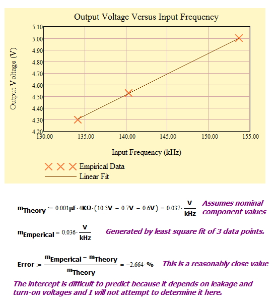
Figure 6 shows 3 data points from a version of this circuit that I am using for a home project. This particular application had C1 = 0.001 µF and R1 = 4 k?. You can see that the response is quite linear, the measured and predicted slopes were within experimental error, and it is working well in my application.


I don't really understand why you are doing -VD1-VBE1 in figure 2, those voltages are in a closed loop.
This is not a closed-loop feedback system. While there is a transistor in the circuit, it is really used as a current switch. This circuit is really a form of diode switching network, so the voltage drops (diode and base-emitter junction) must be accounted for.
mathscinotes
Thanks for replying, I ended up understanding that part, here is a more detailed explanation (just in case someone is looking for one):
When V2 is low C1 will charge through D1. Assuming that V2 remains low for a longer time than what it takes C1 to fully charge, then the final voltage drop across C1 will be of V1-0.7V (due to the diode biasing), after that the diode stops conducting and we have to "wait" for V2 to go high. During this time Q2 is not conducting since Vb = V1 > Ve = V1 - 0.7 V.
When V2 goes high then Vb is still V1, but Ve is now Ve = V1 - 0.7 V + V2 (but V1 and V2 are equal (12 V) when V2 is high). So now we have: (Ve)initial=2 V1 - 0.7 V > Vb= V1. So Q2 will conduct and C1 will begin to discharge through R1 while charging C2. Assuming that Q2 is saturated then Vce is approximately 0 V (not really). So Q2 will conduct until Ve-Vb reaches the forward biasing requirement of the transistor, which I assume is 0.7 V. So we have: (Ve - Vb)final = V1 + Vc1 - Vb = Vc1= 0.7 V .
Since (Vc1)initial = V1 - 0.7 V, and (Vc1)final = 0.7 V then the total charge that must go through the output is (V1 - 1.4 V)*C1. But initially C2 and R1 behave as a short circuit, so the whole charge is quickly stored in C2. If all that charge went to C2 then it would translate in (V1 - 1.4 V)*C1/C2 = 0.1 V. Since the time constant of R1, C2 is 1 second and the input period is smaller then the output voltage will being to increase in time and we have to wait.
To see why the charge stored in C1 will quickly be transferred to C2, even as the voltage increases consider the following:
Once the transistor opens almost 12 V (V2 + Vc1) must fall through C2 and R1, but initially the voltage across C2 and R1 is less than that (at least for this range of frequencies). The only way to satisfy that is if C2 is suddenly charged to 12 V, but that won't happen since the transistor will close first, remember from before that the maximum change in voltage that each pulse can make in C2 is 0.1 V.
That explains why the opening and closing of the transistor must be fast (like a shortcircuit). But to understand why almost the whole charge will also be stored in C2 and not lost through R1 you have to take into account the values of them:
let's say the charge in C2 increases by q during a time t, then the necessary charge q1 through R1 needed for that will be:
R1 * q1 / t = q / C2
From before we know t will be very short, and C2*R1 = 1 s which is much higher than time t. So q1 has to be very small compared with q.
Finally equilibrium will be reached once the voltage given to C2 is such that the same voltage will be lost during the time the transistor is off (which is almost T, remember that the charging is very fast, as soon as V2 goes high). That means:
[ (V1 - 1.4 V)*C1/C2 ] = Vout*(T/(R1*C2))
where Vout is the equilibrium voltage through C2 (and R1), and T/(R1*C2) is the off time relative to the discharge time (the real solution is proportional to exp(-t/(R1*C2)) and this is what you get after expanding in series around t=0).
C2 cancels because the voltage through it goes up as C2 goes down, but as C2 goes down the discharge time constant goes down.
Excellent description.
mathscinotes
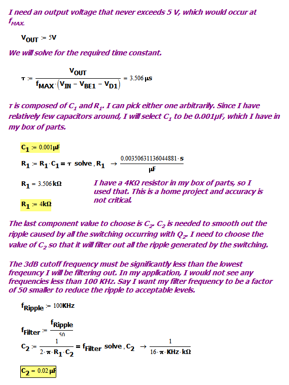
How did you come up with the valeus of c1, c2 and r1? could you pls show me the formulas you use. thank you in advance.
Hi Charles,
I will include a modified version of my post here that will focus more on the tradeoffs associated with component selection.


Thank You very much for this. I will be using your circuit in order to sense a capacitance in the range of femto F. This would really help me a lot.
Thanks dear... it was really helpful.
I just ordered som ICs to perform just that but I was still seaching for a more simple solution with discrete components. So thanks for this elegant solution.
In my testing, I used a 555 timer to get the frequency ( 1-3 kHz at 5V) and hooked it to your circuit. I immediatly noticed a linearity issue when changing the frequency. A change by a factor 3 in frequency only resulted in a drop of 1 V. I tuned the circuit to ouput approx. 5V at max so I should have obtained less than 2V after the change. I solved that by putting a 1K resistor in series before C1. It causes a drop of 1 V on the input of the converter circuit but it also restores the linearity.
On a side note : the final goal is to convert the output of a capacitive sensor ( rain detector) into a voltage signal. The sensor controls the frequency of a 555 timer in astable mode and the square wave is converted to a voltage that is linearly changing with the capacitance of the sensor. This works quite well.
On a side note bis: I also noticed on the scope a high frequency noise content on the output of the 555 timer when it was hooked to the converter circuit. Not sure why it does that.
Just a follow up : this is what happens when you go in a forum/comment section explaining an weird issue before considering every possible trap. You look like a complete idiot. So in the end, nothing was wrong with the F to V converter, it was a decoupling cap wrongly connected on the 555. Once set right, no more noise and no linearity issue.
I'm glad it worked for you. I like what you were doing with your rain gauge sensor and I plan to build one once the water here unfreezes.
mathscinotes
Hi, when V2 goes high then we have Ve=2V1-0.7 and Vb=V1, that makes Veb=V1-0.7 , because Veb can't go that high, then there is a quick discharge from C1 to get aprox. Veb=0.7, so C1 have to discharge instantly V1 volts (with a time constant depending of the internal resistance of V2 and the transistor's emitter base diode )
I . n . g . e . n . i . o . u . s . !
It's surprising to find on mathscinotes.com a resource so precious about equations.
We will note your page as a benchmark for A Simple Frequency-to-Voltage Converter .
We also invite you to link and other web resources for
equations like http://equation-solver.org/ or https://en.wikipedia.org/wiki/Equation.
Thank you ang good luck!
hi, I have a question that puzzles me for several days. How can I know the time to arrive at the point of equilibrium of Vout. Because when I simulate the circuit shown in the fig.2, there always takes a period of time before the Vout arrives at the point of equilibrium. And can the time be controlled?
I experienced the same when I modeled the circuit exactly in LTSpice. Using the inventors original values it takes three seconds before the output reaches equilibrium.
Although the linearity is very good when I graphed the output, the output voltages are not the same as what the inventor's showed.
if anyone can anyone give me links or just a list off the parts needed it would be much appreciated thanks 🙂
And/Or a photo of a completet circuit would be soo nice. I'm not realy getting this just from the schematics. Sorry :/
Hi, I don´t have the technical knowledge to build this on my own so my question is if there are any cheap alternatives online with a similar output? Preferably with a little bit higher output voltage and a dial to adjust the output.
Before I say anything please understand I am new into the field of electronics. I just want to clarify that the input frequency should be the "Sensor Interface Output" and the "Supply Voltage" is just an outside voltage source. Also is the Vout located on the top wire? Probably being stupid but I just want to make sure I have the right idea of how this works.
what a moron
Thanks for 'Simple Frequency-to-Voltage Converter'.
Thank you for simple yet effective FV converter.
There is simulation: http://www.falstad.com/circuit/circuitjs.html?cct=$+1+0.000005+0.529449005047003+56+5+50R+128+144+128+208+0+2+1000+3+0+0+0.5v+272+288+272+224+0+0+40+3.3+0+0+0.5t+352+176+400+176+0+-1+3.1258328488407208+-0.35676374006289+100c+192+144+256+144+0+3.0000000000000004e-9+-6.65676374006289c+400+240+400+288+0+0.000009999999999999999+0.17416715115927917r+448+240+448+288+0+2000d+272+224+272+144+2+defaultg+272+288+272+320+0w+128+144+192+144+0w+256+144+272+144+0w+400+160+400+144+0w+400+144+256+144+0w+352+224+272+224+0w+400+192+400+240+0w+400+240+448+240+0w+400+288+448+288+0w+352+176+352+224+0w+400+288+272+288+0o+5+64+0+4618+1.25+0.0125+0+2+5+3o+8+64+0+36878+5+51.2+1+2+8+3
It's easy to pick values in the simulation for particular voltage and frequency requirements.
I think the link is broken. Could you fix it?
Which link is broken? I tried all I could see and they worked.
mark
I meant the link from igrowing's comment. He did an online Simulation. And this link is broken.
http://www.falstad.com/circuit/circuitjs.html?cct=$+1+0.000005+0.529449005047003+56+5+50R+128+144+128+208+0+2+1000+3+0+0+0.5v+272+288+272+224+0+0+40+3.3+0+0+0.5t+352+176+400+176+0+-1+3.1258328488407208+-0.35676374006289+100c+192+144+256+144+0+3.0000000000000004e-9+-6.65676374006289c+400+240+400+288+0+0.000009999999999999999+0.17416715115927917r+448+240+448+288+0+2000d+272+224+272+144+2+defaultg+272+288+272+320+0w+128+144+192+144+0w+256+144+272+144+0w+400+160+400+144+0w+400+144+256+144+0w+352+224+272+224+0w+400+192+400+240+0w+400+240+448+240+0w+400+288+448+288+0w+352+176+352+224+0w+400+288+272+288+0o+5+64+0+4618+1.25+0.0125+0+2+5+3o+8+64+0+36878+5+51.2+1+2+8+3
Got it! I will try to fix it.
biegert
Sorry about this. I didn't check the link.
As alternative, you can go http://www.falstad.com/circuit/
And paste the circuit text via File -> Import from text...
$ 1 0.000005 5.934295036739208 56 5 50
R 176 176 64 176 0 2 10000 3.3 0 0 0.7000000000000001
c 176 176 240 176 0 1e-8 0.1299108276163885
c 400 288 400 352 0 0.00001 3.7354801206917565
r 464 288 464 352 0 1000
d 272 256 272 176 2 default
t 352 192 400 192 0 -1 -0.4354801206917567 0.1299108276163885 100
g 336 352 336 384 0
v 208 352 208 256 0 0 40 3.3 0 0 0.5
w 400 208 400 288 0
w 272 256 208 256 0
w 208 352 336 352 0
w 336 352 400 352 0
w 400 352 464 352 0
w 464 288 400 288 0
w 352 192 352 256 0
w 352 256 272 256 0
w 400 176 272 176 0
w 272 176 240 176 0
o 0 2 0 4614 5 0.1 0 2 0 3
o 3 128 0 4610 10 0.1 1 2 3 3
Hi, I am trying to make this cuircuit for a college work and I would like to know what are the components of this project, especially the "Sensor Interface Output" and any good advice on building this.
I am very new to electrical work and was wondering if there were to be a tutorial in setting up this circuit, any help will be appreciated
Pingback: DIY LED Music Visualizer | Real-Time Animations (Arduino) – Miftah Steven Code
Is there a good way to use this for a soundwave and output it with 5v max so it can be used with an arduino?
I would also like to know this if Mathscinotes could come to the rescue!
I've been trying to build the circuit to read in an audio signal. For a 5V Arduino I'm assuming the signal would have to to be amplified but would it need to oscillate around +2.5V as well rather than 0V so that there's no negative voltage? Then I'm guessing the output of the amplified & offset audio signal would simply connect to C1?
Any help would be much appreciated as my electrical engineering has faded quiet a bit since college.
It's a work of art, what are the component values you used
What would be the frequency range of such a circuit? I want to build an audio to control voltage interface to convert audio output from a keyboard into a control voltage for an analog synth. I realize that non-linearities may sound out of tune, but not to worry for now. My concern is the range of the conversion. I would need something like 100hz-4khz to get a few octaves. Can you suggest capacitances that would support this in your circuit?
Thanks for a great design by the way.
Tony
Does this circuit also work for sine waves?
How do you change this circuit to accept frequencies between 0 to 100kHz?
That's why maths is known as the mother of science
Hi,
Came here from Devon Crawford's video.
That is a very good site. Thanks for mentioning it!
mark
Hi, thank you for sharing. Do you know where to get LTspice models?