Quote of the Day
No. I would either have to embarrass too many people, or I would have to lie. I refuse to do either.
— General George C. Marshall's response when offered $1M to write his memoir on WW2.
Introduction
I have a home project that requires me to design a Schmitt trigger circuit. There are numerous places on the web where you can find design equations for the Schmitt trigger constructed using an open-drain comparator. Unfortunately, these design equations do not model the output low-level saturation voltage of the comparator and in my application I need to be concerned about this voltage. My objective is to determine formulas for the resistors in the circuit as a function of the various threshold and output voltage levels I require.
As I have mentioned before, I met Otto Schmitt (Figure 1) when I was an undergraduate. As one of so many clueless undergraduates, I had no idea who I was talking to when I met him. He just seemed like another kindly old professor at the time. His office was in a decrepit structure called the Temporary Engineering Annex, which were WW2-era buildings that eventually were torn down. As I came to know more about him, I realized what a major league engineer he was. The University of Minnesota is starting to put together a web memorial to him at this location. I did find a pretty good discussion of his life and accomplishments at this web site.
I have been fortunate to meet and be influenced by people like him throughout my life. Hopefully my sons will be able to say similar things about their upbringing and education.
Background
Schmitt Trigger Description
The Wikipedia defines the Schmitt trigger circuit as
A comparator circuit with hysteresis, implemented by applying positive feedback to the non-inverting input of a comparator or differential amplifier.
Comparators are circuits that make decisions − they decide a one voltage is larger or smaller than another voltage called the reference or VRef. In a noise-free environment, these decisions would be unambiguous. However, the real-world is full of noise and this noise can make the comparator output toggle wildly when input voltage is near VRef. This noise-stimulated toggling is usually a problem for the circuits monitoring the comparator output. The Schmitt trigger is designed to alter its reference level after the output switches so that noise will not cause further switching.
Figure 2 shows the output versus input characteristic of an inverting Schmitt trigger circuit. Notice how positive-going signals will have their threshold level lowered and negative-going signals will their threshold level raised.
Some Definitions
Here are the variable definitions used in my analysis.
- Comparator threshold voltage for positive-going signals.
- Comparator threshold voltage for negative-going signals.
- Output high-voltage from the comparator. Since I am using an open-drain comparator, the output high-level voltage is determined by the external resistor network.
- Output low-voltage from the comparator, which is often referred to as the negative saturation voltage or just saturation voltage.
- Supply voltage for the circuit. This will be a single-supply Schmitt trigger.
Analysis
Schematic
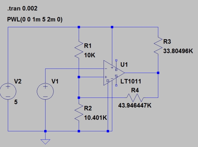
Figure 3 shows a schematic for a Schmitt trigger circuit using an open-drain comparator.
Calculations
My calculation objective is create formulas for each of the resistors in the circuit as a function of the my critical voltage specifications, which are ,
,
,
, and
.
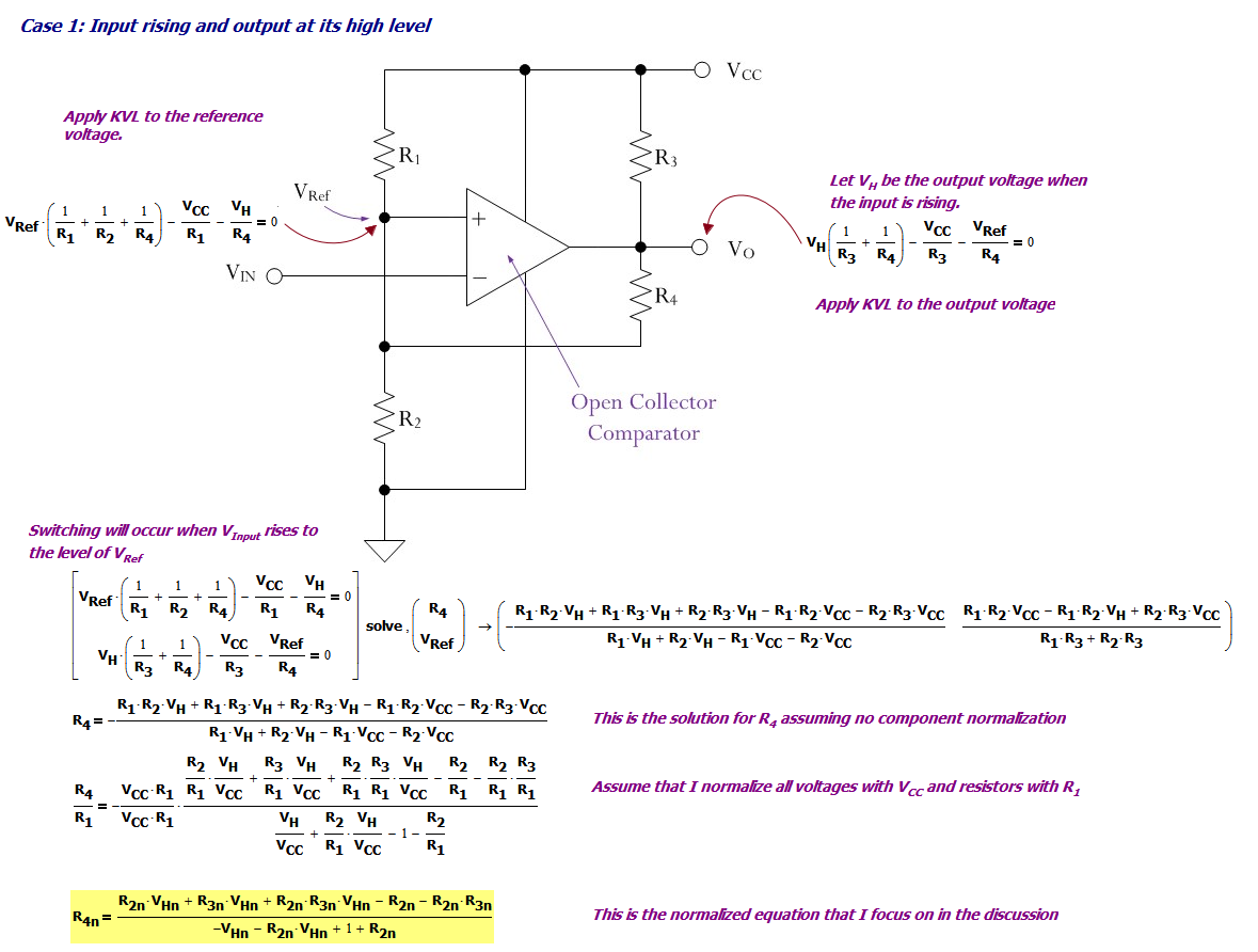
Because there are so many variables (5), I have chosen to normalize my calculations. In this case, I will express all the voltages relative to VCC and all resistors relative to R1. This reduces the number variables down to three, which is more manageable. My graduate school adviser, Aram Budak, would always chastise me when I carried around unnormalized variables in my calculations. He said the extra work was simply not worth it, and he was right. For those who want to see a more conventional derivation, see my response to a question at the bottom of the post.
I begin my calculations by expressing R4 in terms of my voltage specifications (see Figure 4).
In Figure 5, I now setup a system of equations that will give me the equations that I need to compute my normalized resistor values.
Figure 6 shows a worked example. Notice how I normalize all the voltages before I insert them into my formulas and then I need to unnormalize the results.
Simulation
Before I build a circuit, I always like to simulate it. Here are my LTSpice results for this circuit.
Schematic
Figure 7 shows the circuit I simulated.
Simulation
Figure 8 shows my simulation results. My critical voltages are exactly what I wanted because my equations allowed me to model the finite output voltage of the comparator when in the "low" state (~0.152 V).
Conclusion
In this blog post I designed a simple Schmitt trigger circuit for use in a home project. As part of this effort, I was able to derive equations for the associated resistor values in terms of the normalized transition and output voltages. My equations allow me to account for the non-zero output voltage of the comparator when it is in the "low" state. I simulated the circuit using LTSpice and I showed that it worked as I expected.


Pingback: A Simple Frequency-to-Voltage Converter | Math Encounters Blog
Please explain how did you find out the first equation?
Vh * (1/R3 + 1/R4).... ? Where is it com from? This is Kirchoff's 1-st law? With the node at Vo?
Hi Rad,
I am sure this was confusing. I was using this post to train some staff on using normalized component values and it probably was too much for a blog. Here is a derivation of the R4 equation with no normalized values and then I show how to get the normalized formula.

Thank you.
And WOW. I need take closer look on MATHCAD. Solving this equations on paper will be just too much time consuming.
Thank you again.
Mathcad is a very good tool – I have a strong preference for it when doing routine engineering calculations. However, it is expensive and takes a bit of work to learn to use. Remember that watching people skilled in the use of any tool can leave the impression that using the tool is easier than it is.
There are other free tools you might start with to see how you like symbolic algebra programs. I have used Macsyma and it works very well. The output is not as pretty, but the results are very good. I have experimented with Smath (free also) and gotten some good results too.
At home I use Mathematica, which is extremely powerful (more powerful than Mathcad) but also expensive. However, the output is not quite as nice as Mathcad for blogging and general documentation. I use Mathcad for blogging because I generally write over lunch at work and we use Mathcad at work. I picked Mathcad for work use because training engineers in its use is easier than for Mathematica.
mathscinotes
Pingback: Comparator – some math / Komparator – trochę matmy | DareIT
Hi, is there a way to adjust the value of VL?
Your simulation showed a square signal from 0.152 V to 4V, is it possible to tweak it to, for example, 1.4V to 4V?
If your talking about the output of the Op Amp then you can add a resistor to the negative voltage controll (ground in this case) and it wont drop as low.
The low-level is set by the output impedance of the comparator's output transistor. This circuit does not provide you that kind of control. Other circuit configurations will do what you want. If I have time, I will think about alternatives.
mathscinotes
Hello Mathscinotes,
Did you find any solution? Even I am looking for the circuit,tried a lot not able to figure it out.... I want high-level 8v and low-level 2v. I am able to get one at a time.
If you wish to set the low output level, you need to add a resistor. For the circuit in the post, the output low voltage is not controllable – it is set by the comparator output level. Take a look at this pdf.
I also decided to write a post on the subject.
mark
Pingback: Open-Drain Comparator Circuit With Settable Trigger and Output Levels | Math Encounters Blog
Pingback: Open-Drain Comparator Circuit With Settable Trigger and Output Levels | Math Encounters Blog
How we can design a schmitt trigger when we don't have information about upper and lower bands, we only have information of Inductor current 1Ampere and Inductor ripple current as 0.2A?