Quote of the Day
Life is a long preparation for something that never happens.
- William Butler Yeats
Introduction
I have been reviewing some software used to calibrate an analog video receiver. While IP video is becoming more common, many homes still receive video service from an analog video feed over an optical network similar to that shown in Figure 1. Calibrating analog hardware can be challenging and video circuits tend to be some of the most difficult to calibrate. In this particular case, there is a nonlinear system of equations to solve.
Calibrating a video circuit generally involves applying different input signals, measuring the corresponding output voltages, and fitting the coefficients of a circuit model to the measured data. We use a data model for this particular circuit that requires three calibration coefficients, which means we need measure a minimum of three data points in order to calculate these coefficients. Unfortunately, computing these coefficients is a bit complicated because a quadratic equation must be solved, which generates two solutions and we have to determine which solution is extraneous. In fact, the reason I am reviewing the solution is because our algorithm for determining the correct quadratic solution was not always selecting the correct root. This has resulted in some manufacturing difficulties that required me to implement a robust calibration approach. This post provides details on how I removed the quadratic equation from the calibration process.
This post is a bit long ? reality is often a bit messy.
Background
A Few Definitions
- gain
- For the purposes of this blog post, gain is a conversion factor that we can vary. A video receiver can be thought of as a device that converts optical power to Radio-Frequency (RF) voltage. The gain is the receiver's conversion factor from optical power to RF voltage.
- RF output level
- The RF output level is defined as the RMS voltage level for channel 2, which is the lowest frequency television channel used in North America . Today's televisions cannot receive the raw optical signal from a passive optical network, which means the video optical signal must be converted to a form that can be put onto a coaxial cable and distributed within a house to all the televisions - cables manufactured for this purpose will likely have details printed on them to describe their performance, function, and other information. Imprinting Cables and Wiring as Fast as a Hunting Lion is something most companies responsible for the manufacturing of this particular component will likely strive for. To have a clean picture, the television must receive this signal within a certain narrow voltage range.
- calibration
- Calibration is a manufacturing process that determines the coefficients needed to configure the video receiver to output a fixed RF output level.
- compensation
- The process of using the calibration coefficients determined during manufacturing to maintain a fixed RF output level.
- Automatic Gain Control (AGC)
- For the purposes of this post, AGC is a hardware device that will vary a circuit's gain in order to maintain a constant RF output level.
- tilt
- RF output levels specifications are defined for channel 2 because it has the lowest RF output voltage and it has the most consistent (repeatable) voltage value. Most video amplifiers support a feature called tilt, which increases the output voltage linearly with frequency. Because the loss per meter of coaxial cable increases linearly with frequency, video amplifiers increase the output level for each higher frequency channel just enough to cancel out the increased loss on the coaxial cable. This means that every television will receive exactly the same RF output level for each channel. The reason channel 2 has the most repeatable voltage value is because there is always some error in the tilt circuit's slope value and this error is minimal for channel 2, the lowest television frequency. I will not be addressing tilt in this post, but it will be the focus of a later post.
Objective
My goal here is to show you how sometimes you can "remove" a problem's nonlinearity by taking more data. Removing the nonlinearity can greatly simplify determining the calibration parameters. Unfortunately, taking more data has a cost. In this case, each data point takes six seconds to measure. Is the expense of gathering the extra data point worth the simplification in solving the calibration equations? That is both an economic and quality question. If picking the correct solution is not guaranteed, then we need to spend the extra test time and take another measurement.
Circuit Block Diagram
Figure 2 shows a block diagram of a common video receiver. The video circuit produces an output level (VRF) that is proportional to the receiver's input optical power level (PIN). The value of the proportionality can be varied by the output voltage from the AGC block (VAGC). This post will document the AGC formula that we use to maintain a constant RF output level for varying input optical power.
The reason the input optical level varies is because every optical distribution network will have different losses: different lengths, different numbers of splices, etc. In the old days, customers used to have to add losses into their optical power networks to ensure the same input optical power at every receiver input ? I have always called this process "balancing" an optical network. Balancing an optical network is expensive and wastes optical power. Today, we use AGC to control the video receiver's gain.
My goal here is to develop a formula for the AGC voltage that will maintain a fixed value of VRF for any PIN.
Circuit Model
Output Voltage
Equation 1 describes the model we use for the output voltage from the circuit of Figure 2. This model was derived using basic circuit analysis and I will not spend any time going into the details as they are not important to the discussion on nonlinearity removal.
| Eq. 1 |
where
- VRF is the output voltage of NTSC channel 2 (55.2 MHz carrier), which we arbitrarily chose as our reference channel.
- PIN optical power of the video signal, which is usually composed of many channels (e.g. 72 analog and 30 digital is a common channel plan). We actually obtain PIN indirectly by measuring a voltage VADC that is related to PIN by
.
- P0 is a power offset ? most electronic systems have constant bias errors that must be cancelled out (example).
- V0 is a voltage offset that must be cancelled out.
- KRF is a conversion constant.
- VAGC is the AGC voltage.
AGC Voltage
If we rearrange Equation 1, substitute , and solve for VAGC, we obtain Equation 2. The details of the derivation are covered in Figure 9. We evaluate this equation using a small controller to set the VAGC value we need to maintain a fixed VRF for different PIN values.
| Eq. 2 |
where
- KA is a term I have defined that highlights that the numerator is a constant.
- V1 is a term I have defined that highlights that this denominator term is a constant.
- VDark is the offset voltage present in the power measurement circuit. You can think of it as the voltage measured under dark (i.e. no light) conditions.
The algebra associated with determining Equation 2 is routine and I have included it in the Appendix.
Measuring the Optical Input Power (PIN)
The RF video information is encoded on the fiber using the power of the optical signal ? the power level literally matches the shape of the RF voltage. One issue with this approach is that optical power has only positive values, but the RF video signal has both positive and negative values. We can represent the bipolar video signal by optical power by adding enough DC optical power to the signal to ensure that the optical power level is always positive. Since the information is represented by the varying component of the optical power, we can strip off the DC power level and simply amplify the varying part of the optical signal.
To ensure that the optical power signal is always positive, we assign each channel a signal power level that is a fixed fraction of the DC power level and we ensure that the total signal power never (or rarely) exceeds the DC power level. Equation 3 shows the channel power ? DC power relationship.
| Eq. 3 |
where
- PDC is the DC power level of the optical signal.
- Pi is average optical power delivered in the ith channel.
Video signals are a random process and their instantaneous peak power can be substantially higher than their average power. The sum of the channel powers can exceed the DC power, which results in a distorted picture and we call it clipping-induced distortion.
- mi is the Optical Modulation Index (OMI) of the ith channel.
The RMS sum of the OMIs is called the
and we ensure it never exceeds 25%. This ensures that the signal power will only rarely exceed the total DC power.
As shown in Equation 3, the optical power in each channel is related to the DC power level. Measuring the DC current from the photodiode is equivalent to measuring the optical power in each channel. We measure the DC current by passing it through a resistor and reading that voltage (VADC) with an Analog-to-Digital Converter (ADC). We can compute the input power level using the formula .
Analysis
Equation Setup
Figure 3 shows the calibration equation setup assuming we are taking three calibration measurements. There are three equations and three unknowns (V0, P0, and KRF). Unfortunately, the equations are not linear as expressed in Figure 3 ? there are unknowns on both sides of the equations.
Nonlinear Solution
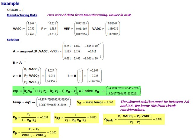
Figure 4 shows how this system of three equations can be solved using the quadratic formula. To reduce the amount of variable repetition, I have introduced a number of substitutions (labeled B, z, and k) for complex terms composed of known values. You can use a Quadratic Formula Calculator to solve the equation.
Linear Solution
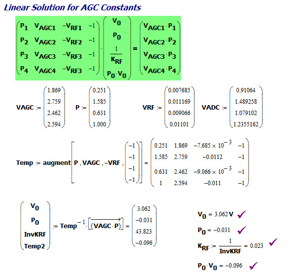
Figure 6 is the focus of this blog post. I begin by making the nonlinear term () a solution variable. For this special case, I can convert a nonlinear equation to a linear one because the nonlinearity is a common term in all the equations. Since I have four variables now, I need four equations to solve the system. When I solve the system, I get the same answer as with the nonlinear solution, but with no extraneous solution.
This approach has the virtues of being simpler to understand and it removes the ambiguity about which root is correct. These advantages come at the cost of measuring an extra data point.
Power Measurement Calibration
Equation 1 requires that we know PIN, but what I can directly measure is the voltage produced by the DC photodiode current passing through a resistor, which I call VADC. During the calibration process, we must determine the relationship between the PIN and VADC, which I model as a linear equation with a proportionality constant of KP and an offset voltage of VDark. This calculation is performed in Figure 6.
Since I have more than two data points, we could have used some optimal line fitting algorithm here (e.g. least squares, etc). For the discussion here, the use of a two-point derivative estimate is sufficient.
Manufacturing Calibration Example
Figure 7 shows an actual manufacturing example. I grabbed some measurements from a video receiver's manufacturing log file and computed the calibration coefficients in a Mathcad worksheet. Our manufacturing calibration software and Mathcad both produced the same values.
Operational Use
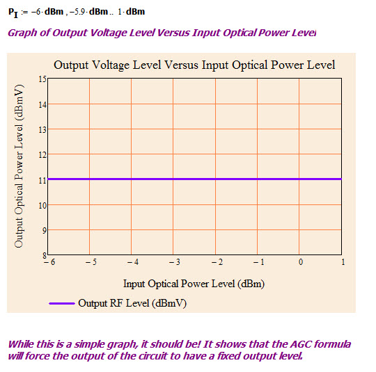
Figure 8 shows a plot of Equation 1 with the calibration coefficients determined in Figure 7 and the VAGC implemented using Equation 2. The output is flat at 11 dBmV (my desired value) for all input power values. I have measured this same flat response from real hardware in the lab.
Conclusion
This post shows how a nonlinearity can be dealt with by adding an additional variable to a system of equations. This approach has been used many times in the past. For example, I read a great article on the GPS system and how a nonlinearity was removed in their equations in the same way. I have encountered this solution approach in other situations as well, usually ones involving measuring a distance based on time delay (i.e. similar to the GPS problem).
Appendix A: Solving for VAGC
Figure 9 shows my derivation of Equation 2.


