
Quote of the Day
Torture the date, and it will confess to anything.
— Ronald Coase, data scientist
Introduction

Figure 1: Examples of Filter Roll Offs. (Source)
During a recent circuit design review, I saw the need for a simple two-pole filter in one region of the circuit. As I thought about, this filter might be a good example to work through here in the blog. While the application is rather routine, it does illustrate the general process involved in designing one of the most common forms of a low-pass filter.
This is also good application for a computer algebra system. I chose Mathcad, which did a very nice job.
Requirements
I am constantly amazed at how many people try to "short-change" the amount of effort they spend on determining requirements. I make sure that I have the requirements fully determined before I start designing. As far as I am concerned, every minute spent working on the wrong problem is a minute wasted.
This does not mean that determining requirements is easy. I refer to this process as "The Treasure Hunt." Requirements are my treasure and, like any real treasure, you may have to look hard to find it. In this case, the requirements were pretty obvious:
- The output of the filter is a quasi-DC voltage level (i.e. it changes slowly and infrequently)
We are using the PWM generator followed by this filter to build a "poor man's" a digital-to-analog converter (DAC). We are working with a very low-cost device that has a PWM generator but not a DAC. Our cost goals are so tough that we cannot afford to add a DAC. - The input to the filter is a pulse train that is pulse-width modulated.
As mentioned above, we have a PWM generator available for free and we want to re-task it for use as a DAC. - The input level is from 0 to 1 V with a modulation rate of 100 kHz.
The PWM generator uses 100 kHz switching frequency and we need to filter this component out to achieve a smooth enough DC level. - The output level is from 0 to 5 V and is to be a DC level with less than 0.5 mV of ripple.
We need a relative steady voltage level. With an input amplitude of 1 V and an output amplitude of 5 V, it also means we need a circuit with some gain. - The circuit is not sensitive to offset voltage or any of the other op-amp imperfections.
Some applications are very sensitive to common-mode errors, offset voltage, or bias currents. This application in not one of those.
Design
Approach
Given the operational requirements listed above, we can derive some design requirements as shown below.
- I need to attenuate the PWM-induced voltage ripple by at least 4 orders of magnitude (5 V/10,000 = 0.5 mV).
- Attenuation by a factor of 10,000 means 80 dB of attenuation
.
- As a working assumption, set fBW = 100 Hz.
This means we will have 3 decades of frequency rolloff to reduce the filter gain down by 80 dB or more. A wider transition region reduces the order of the filter required. - A 2-pole filter should provide more than enough attenuation.
A 2-pole filter provides 40 dB of attenuation per decade of frequency rolloff. A 2-pole filter should be able to meet 80 dB of attenuation over 2 decades of frequency rolloff. Since we have 3 decades of frequency rolloff to work with (100 Hz to the 100 KHz PWM frequency), I should actually see 120 dB of attenuation (more is good). So I will set the filter bandwidth at.
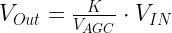
- The circuit needs a gain of 5 at DC (0 Hz)
Basically, the circuit will need to amplify a pulse train with a 1 V peak amplitude to a DC level with a 5 V peak amplitude. - The circuit needs to have a low output impedance.
This means that I really would like to have the voltage come directly off of the output of an opamp.
The circuit does not have stringent transient response requirements. I just need a nice, stable, filter circuit (i.e. no high Q poles). In this situation, many engineers will choose a Sallen-Key circuit configured to implement a Butterworth filter. That is exactly what I will do here.
Butterworth Polynomial
Implementing a Butterworth filter means coming up with a physical realization of a Butterworth polynomial. Normally, I just read the polynomial from a table. For illustrative reasons, I will forgo the table look-up and will derive the second-order Butterworth polynomial using the key defining characteristic of a Butterworth polynomial – maximal flatness at 0 Hz.This same approach can be used to determine the Butterworth polynomial of any order. I will also show any other Butterworth polynomial can be found.
Maximal flatness means that the first n-1 derivatives of the magnitude-squared function 


We can set the first n-1 derivatives to zero because (1) we have n coefficients (i.e. n degrees of freedom), and (2) we use one degree of freedom when we set 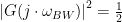
Equation 1 shows the general 2-pole, low-pass, magnitude-squared function.
| Eq. 1 | 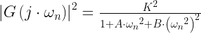 |
where
- K is the gain at 0 Hz (5 in this case).
- A, and B are polynomial coefficients.

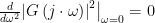
In Figure 2, I use Mathcad's symbolic solver to show that A = 0 and B = 1.

Figure 2: Derivation of the Magnitude Squared Function.
In Figure 1, we derived the magnitude squared function 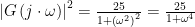

Figure 3: Derivation of the Second-Order Butterworth Polynomial.
Thus, the second order Butterworth polynomial is 
We can prove that the general form of the magnitude-squared form of a Butterworth Polynomial of order n is 

Figure 4: Mathcad Program for Generating a Table of Butterworth Polynomials.
Sallen-Key Circuit
Figure 5 shows the Sallen-Key circuit, which is a very commonly used circuit for this type of application.

Figure 5: Sallen-Key Low-Pass Filter Circuit.
I have used this circuit many times with much success.
Analysis of Sallen-Key Circuit
Figure 6 shows a standard Kirchoff's Voltage Law (KVL) analysis of the Sallen-Key circuit.
Standard Solution

Figure 6: Equations for the Sallen-Key Circuit.
I usually do not work with filter equations in the form shown in Figure 5. I like to normalize the frequency variable, s, relative to the filter bandwidth (
Normalized Form
Figure 7 shows the Butterworth equation normalized to the filter bandwidth. This is the equation form normally shown in the filter design tables.

Figure 7: Development of the Normalized Form of the Butterworth Filter.
Component Determination
Figure 8 shows how we can determine the component values required for this implementation using the equation solving abilities of Mathcad.

Figure 8: Determination of the Passive Components Value.
We can now generate a plot of the filter magnitude characteristic using these component values.
Gain Characteristic
Figure 9 shows the gain characteristic of this design. As expected, we are seeing 120 dB of ripple attenuation. The gain at 0 Hz is 5, so that requirement is also met.

Figure 9: 2-Pole Butterworth Gain Characteristic.
Conclusion
This was a good example of a common filter design problem. I have used both circuit simulators and computer algebra software to design these filters. I have come to like computer algebra software for this kind of work because it gives me equations. These equations allow me to see how the output varies as a function of individual component values. This means that I can see useful approximations.


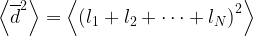
 , that a random walker travels from its point of origin is given by Equation 1.
 is the mean distance traveled.


 can then be computed by assuming the photon traveled a distance of
  at a speed of c. For our rough analysis, we will assume that the average free path, l, for a photon is ~1 cm. Determining this number is complicated and I will refer you to this


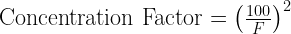
 , where f is the focal length and DLens is the diameter of the lens. For the lens in their example, they computed an F-number of about 3.16, which means the concentration factor is 1000. This means that the power at the spot is the same as what entered the lens, but it is concentrated on an area 1000 times smaller.

 , where Ө is the angular diameter of the Sun.


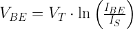
 from the
 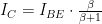 , where ? is the current gain of the transistor. Equation 1 models this characteristic very well, particularly at low currents.
.")
 . Since maximizing the logarithm of the power is the same as maximizing the power, we can maximize this equation and obtain our objective.
 .
.
 .
.
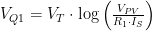
 . To derive this equation, note that the minus input of A1 is a virtual ground. This means that the voltage across R2 is
  . From this voltage and the value of R2, we can compute IQ2.
 .
.

 is the power from the solar panel.


 , where K0 is a constant? The result is shown in Equation 2.


 and
and  .
.


