Current Source Built with a Negative Resistance

Introduction

I have seen quite a few schematics lately that are using an operational amplifier (opamp) configured as a negative resistor. I thought it would be interesting to analyze this circuit and show how it can provide an economical solution to a common sensor interface scenario.

Background

Figure 1 illustrates a common sensor interface scenario. This scenario consists of:

  • Sensor
    The sensor has a resistance characteristic that varies according to some external parameter, e.g. temperature, ambient light level, gas concentration.
  • Current Source
    A current source drive can be desirable for a number of reasons: (1) The sensor may be calibrated for a specific current level, (2) The sensor may have a linear response for a given current drive, (3) The sensor output voltage range needs to be restricted in some way.
  • Amplifier
    The amplifier is often needed to provide isolation from the monitoring circuitry and to scale the output for further signal processing.
Figure 1: Common Sensor Interface Scenario.

Figure 1: Common Sensor Interface Scenario.

Negative Resistance Opamp Circuit

Figure 2 shows an operational amplifier connected as a negative resistance.

Figure 2: Negative Resistance Circuit.

Figure 2: Negative Resistance Circuit.

Equation 1 shows the derivation of the negative resistance equation.

Eq. 1 {{v}_{I}}={{v}_{O}}+i\cdot {{R}_{F}}
{{v}_{I}}={{v}_{O}}\cdot \frac{{{R}_{1}}}{{{R}_{1}}+{{R}_{2}}}
{{v}_{I}}={{v}_{I}}\cdot \frac{{{R}_{1}}+{{R}_{2}}}{{{R}_{1}}}+i\cdot {{R}_{F}}
-{{v}_{I}}\cdot \frac{{{R}_{2}}}{{{R}_{1}}}=i\cdot {{R}_{F}}\Rightarrow {{Z}_{IN}}\triangleq \frac{{{v}_{I}}}{i}=-{{R}_{F}}\cdot \frac{{{R}_{1}}}{{{R}_{2}}}

Equation 2 shows the derivation of the voltage gain equation.

Eq. 2 {{v}_{I}}={{v}_{O}}\cdot \frac{{{R}_{1}}}{{{R}_{1}}+{{R}_{2}}}\Rightarrow {{A}_{v}}\triangleq \frac{{{v}_{O}}}{{{v}_{I}}}=\frac{{{R}_{1}}+{{R}_{2}}}{{{R}_{1}}}

Introduction

My application example is shown in Figure 4.

Figure 3: Negative Resistance Example Application.

Figure 3: Negative Resistance Example Application.


The basic idea here is to use negative input resistance of the opamp circuit to cancel out the resistance of RS. Figure 4 illustrates this source transformation.
Figure 4: Source Transformation.

Figure 4: Source Transformation.


The parameters of this case are the following:

  • V_{CC} = 10 V
  • I = 1\text{mA}
  • A_v = 10

Figure 4 shows my solution in Mathcad.

Figure 5: Example Solution in Mathcad.

Figure 5: Example Solution in Mathcad.

Conclusion

I worked through some basic design equations for the application of a negative resistance circuit to a sensor interface example. I have been seeing this circuit quite a bit lately and it is an interesting application of basic linear circuit analysis.

Posted in Electronics | Comments Off on Current Source Built with a Negative Resistance

Engineering as a Social Activity

I haven't been able to blog the past week because I have been in Los Angeles at the Optical Fiber Communication Conference and Exposition (OFC). I always enjoy going to this conference. After thinking about it, I enjoy it because of the people. The optics business is really a relatively small community of people that I have come to know and appreciate over the past 11 years. One nice aspect of this community is that it is composed of very smart people, which helps to keep me at the top of my game. I constantly marvel at the cleverness of the work being done in fiber optics. I also like being a part of a community that is making a real difference in the quality of people's lives. The information revolution has been driven to a large extent by the ability of people to move data rapidly around the world, which mean fiber optics. My association with this community has allowed me to meet people from around the world and to travel to places that I would probably never have seen otherwise. As always happens, a number of mathematical items popped up during the show. I will be writing about these items during the following weeks.

Posted in Management | Comments Off on Engineering as a Social Activity

Will Do Math For Free Lunch

Introduction

Engineers and managers at manufacturing companies frequently have sales folks come by who want to take you out for a "free" lunch. There is no such thing as a free lunch. They want to sell you something. Except the other day ...

I had a salesman call me and say that he wanted to go out for lunch with me. I assumed he wanted to sell me something. I had failed to prepare a bag lunch for that day, so I decided to take him up on his offer. He stopped by the office and picked me up to go to a local restaurant. Our conversation started with the usual chit-chat about the weather and family, but the salesman soon changed the discussion to the topic of pulse-width modulation. A number of his customers were asking for symmetric pulse width modulation (PWM) and he was wondering what was symmetric pulse-width modulation and why would anyone care. Now I knew why he wanted to go to lunch -- he wanted PWM training. As engineers have done since Imhotep designed the pyramids, I pulled out a pen, grabbed a napkin, and the lesson on PWM started.

Background

My history with PWM goes way back to my days as a sonar systems engineer. We used PWM to drive acoustic amplifiers. It was as sonar systems engineer that I learned the hard way about the difference between symmetric and asymmetric PWM. I will explain how I learned the hard way later. In my current position, we use PWM to set voltage thresholds that need to vary under computer control. These voltages are really quasi-DC levels and the symmetry of the PWM drive does not matter. This shows you that the type of PWM you require depends on your application.

PWM Basics

The Wikipedia has a good discussion of the basics of PWM. PWM is often used with power amplifiers whose output level is determined by the pulse width of its input drive. The output amplifiers or the loads they drive often have bandpass frequency characteristics that filter out any high and low frequency distortions introduced by the amplifier, but will not filter out frequency distortions near the PWM carrier frequency. This is the case with sonar systems. It also is the case with many motion control systems.

Symmetric PWM

People care about PWM symmetry when they care about the frequencies coming out of the output amplifiers. In a nutshell, a symmetric PWM drive will not produce frequency components other than the fundamental frequency of the PWM pulse train. Figure 1 illustrates the ideal situation.

Figure 1: Example of an Ideal Symmetric PWM Situation.

Figure 1: Example of an Ideal Symmetric PWM Situation.


Observe how the pulse train input drive is filtered by by the frequency characteristic of the power amplifier and load to put out a pure sinusoid. Figure 1 also shows that the centers of the PWM pulses align with one another, hence the term symmetric PWM. Unfortunately, generating a symmetric PWM pulse stream is more work than for an asymmetric stream. This was a bigger deal with the FPGAs of the Late Stone Age that I had to work with. Modern FPGAs laugh at circuits like this.

Asymmetric PWM

The easiest form of PWM to implement is asymmetric. All you need is a simple loadable counter that restarts counting at a regular interval. Figure 2 shows an example of an asymmetric pulse stream and the sinusoidal output it produces. Notice how the sinusoids are phased shifted with respect to one another. The phase of the output sinusoid varies with the PWM pulse width. This means that our output has a time-varying phase. A time-varying phase is the equivalent of a frequency shift (see Equation 2).

Figure 2: Example of an Asymmetric PWM Situation.

Figure 2: Example of an Asymmetric PWM Situation.

A Simple Example

To illustrate the issues associated with asymmetric PWM, consider the case of an application requiring a sinusoid modulated with a sawtooth output amplitude (Figure 3). A modulated carrier is the norm in sonar and radar systems. Typically, they generate pulses with complex shapes with names like Kaiser-Bessel and Dolph-Chebyshev. However, a simple sawtooth waveform will illustrate the signal distortion issue just fine.

Figure 3: Desired Sinusoidal Output Envelope Variation with Time.

Figure 3: Desired Sinusoidal Output Envelope Variation with Time.


Equation 1 describes the signal that we really want.

Eq. 1 f(t)=A(t)\cdot \sin (\omega \cdot t)

where A(t) is the envelope function.

Equation 2 describes the signal that we really get on the rising edge of the sawtooth. The phase of the sinusoid changes with time. Equation 2 also shows that a linear phase shift with time looks to the outside world like a shift in carrier frequency (\omega \to \omega +k).

Eq. 2 f(t)=A(t)\cdot \sin \left( \omega \cdot t+\phi \left( t \right) \right)
The sawtooth implies a linear variation of phase with time, which we model as k \cdot t during the sawtooth's rising edge.
f(t)=A(t)\cdot \sin (\omega \cdot t+k\cdot t)
f(t)=A(t)\cdot \sin (\left( \omega +k \right)\cdot t)

A similar thing happens when the negative edge of the sawtooth. This introduces a negative frequency offset to the carrier. Both positive and negative frequencies will appear in the output (see Figure 4). Note that the carrier is not present in the output.

Figure 4: Spectrum of Asymmetric-PWM Driven Amplifier.

Figure 4: Spectrum of Asymmetric-PWM Driven Amplifier.

What we really want is what I show in Figure 5, which is a envelope modulated with a single-frequency carrier. You get this with a symmetric PWM drive for the power amplifier.

Figure 5: Time and Frequency Domain Views of a Modulated Sawtooth.

Figure 5: Time and Frequency Domain Views of a Modulated Sawtooth.


Figure 5 shows that the unmodulated sinusoid has a sharp spectral peak and the modulated sinusoid has a slightly broadened peak. Theory predicts the broadening of the spectral peak and the envelope shapes are usually chosen to minimize the broadening.

Conclusion

You care about a PWM signal being symmetric when you care about the frequency content of the output. A symmetric output does not produce the harmonic distortions created by the time-varying phase variation introduced by an asymmetric PWM signal.

I will never forget this lesson. On my first sonar transmitter design, I inadvertently implemented an asymmetric PWM sequence. Since this sonar system was trying to detect faint target echoes, the extra spurs that my asymmetry introduced looked like targets. Fortunately, my implementation used programmable logic and I was able to correct the error quickly once I figured out what was going on. However, the lesson was burned into my brain cells. I shudder just thinking about it even now. It was unnerving looking at a range-Doppler map and seeing false targets appearing where there weren't any. Kind of like looking for a cloaked Klingon Bird-of-Prey. 🙂

Posted in Electronics | 3 Comments

Daily Loss of Solar Mass

Introduction

I occasionally work with customers on using solar power to drive some of their remote optical interfaces. These remote interfaces are used to monitor things like pipelines. In one case, it was used to provide Internet service to a bunkhouse for cowboys where AC power was not available. When I work on these systems, I always find myself amazed at the amount of power that the Sun puts out. Every watt that the Sun puts out comes from fusion, which means that the Sun is constantly losing mass. I started to wonder today about the amount of mass that the Sun must be losing every second. We should be able to compute that. Let's dig in ...

Analysis

As always, we need to gather a little data.

  • Distance from the Sun to the Earth, R= 149·106 km (Source)
  • Solar power density measured at the edge of the Earth's atmosphere σ = 1366 W/m2(Source)

I threw this into Mathcad to get the following result.

Figure 1: Solar Mass Loss Calculation.

Figure 1: Solar Mass Loss Calculation.

So a quick calculation shows that the Sun must be losing 4 million metric tons of mass per second. As a check, I found a similar result through a Google search.

Conclusion

The amount of power that the Sun generates is amazing. The amount of mass it loses per second is also amazing. However, when you look at its total mass (2·1030 kg), the Sun will be here for billions of years to come.

Posted in Astronomy | 2 Comments

Magic Number Analysis - "Money Factor" in Auto Leasing

Introduction

One of my sons is a newly minted accountant. He dreams of someday managing a hedge fund. We spend hours talking about modeling data and making predictions. These discussions have convinced me that I need to know more about financial engineering. To learn more about the subject, I have been watching Youtube videos by the Bionic Turtle. I enjoy these videos because they are informative and short (my attention span is not what it used to be, and it wasn't good even then).

Anyway, the other day I watched a video by the Bionic Turtle on leasing automobiles. Normally, computing lease payments requires using time value of money equations. During the Bionic Turtle lecture, I found that the automobile dealers use an approximation to the time value of money equations that makes their calculations much simpler (i.e. they can be done on a "four banger" calculator). Unfortunately, the video did not go into any detail about the approximation. Since my entire career is a celebration of detail, I could not let this go. 🙂

Kidding aside, I found that deriving the approximation interesting and worth going through here. The derivation involves the creation of a term called the "money factor." Since I do not like "magic numbers" in calculations, I wanted to know where this term comes from.

Note that I do not lease my vehicles. I buy them and drive them into oblivion. My interests here are strictly mathematical. That said, let's dig in ...

Background

Approaches to Lease Modeling

The basic concept of auto leasing is simple:

  • You are using a depreciating asset.
  • The auto dealer expects you to pay for the depreciation.
  • The auto dealer expects to earn a competitive return on his investment.
  • At the end of the lease period, you return the auto to the dealer. He can then sell or lease the used vehicle to someone. Of course, you can decide to buy the vehicle at the end of the lease period.

We can look at the problem from three points of view: future value, present value, and money factor approximation. Fortunately, the future value and present value solutions provide us exactly the same answer. The money factor approximation is useful in that it allows a very accurate loan payment approximation to be computed without having to take numbers to powers. I will go through the math for each point of view.

Pricing

Price is a complex thing when it comes to leasing. For the purposes of this post, I will use four forms of price:

  • PL is the list price.
    Almost no one who buys a car pays list price. Nearly everyone negotiates the price down even a little. I personally have negotiated car prices at "no negotiation" dealers. This is important especially for new car owners who need to ship their cars using a shipping service similar to CarsRelo. The main use of the list price in my analysis here is in determining the value of the car at the end of the leasing period. This is often done as a percentage of the list price.
  • PN is the negotiated price of the car.
    This is the price agreed upon by the lessor and lessee.
  • PF is the amount of money being financed through the lease.
    People who lease cars often have to make a down payment, which reduces the amount of money that is covered by the lease.
  • R is the residual value of the car at the end of the lease. It is often expressed as a percentage of the list price.

Interest Rates

I express the lease interest rate in two equivalent forms:

  • I is the lease's annual percentage interest rate.
  • i is the per payment interest rate.
    Since most leases assume monthly payments, i = \frac{I}{12}.

Analysis

In the following analysis, I will be working through a lease example from this web site. I liked their approach and thought it was a good example. My focus is on explaining the use of an approximation in determining the value of the lease payment.

Future Value Viewpoint

Figure 1 summarizes the derivation of the lease from the future value standpoint. It includes a worked example that shows how to handle the case of making a down payment and negotiating a lower price. As stated earlier, the example is from here. Note that I model the lease payments as an annuity due (information here).

Figure 1: Derivation of Lease Payment Formula From Future Value Standpoint.

Figure 1: Derivation of Lease Payment Formula From Future Value Standpoint.

Appendix A shows the same calculation performed using Excel. The results are identical.

Present Value Viewpoint

Figure 2 shows how the same lease payment formula can be derived from the present value viewpoint.

Figure 2: Derivation of Lease Payment Formula From Present Value Standpoint.

Figure 2: Derivation of Lease Payment Formula From Present Value Standpoint.

Money Factor Viewpoint

This analysis is interesting to me because of its focus on dealing with averages. Here is a summary of the approach.

  • Cars are a depreciating asset. The person leasing the car must pay the depreciation.
  • The total interest paid on the lease is equal to the total payments made minus the amount financed (PF).
  • The amount of the payment is equal to the average interest paid per payment plus the average depreciation paid per payment.

We can summarize the last bullet with Equation 1.

Eq. 1 P={{P}_{I}}+{{P}_{D}}

where

  • P is the monthly lease payment
  • PI is the average interest paid per lease payment
  • PD is the average amount of depreciation paid off per lease payment

We can calculate the average depreciation paid per payment as shown in Equation 2.

Eq. 2 {{P}_{D}}=\frac{P_F-R}{N}

Determining the average interest paid per payment is a bit more complicated. The keys to determining this relationship are:

  • P=\frac{i\cdot \left( {{P}_{F}}\cdot {{\left( 1+i \right)}^{N}}-R \right)}{{{\left( 1+i \right)}^{N}}-1}
  • Use of the Taylor series substitution {{\left( 1+i \right)}^{N}}\approx 1+N\cdot i+\frac{{{N}^{2}}\cdot {{i}^{2}}}{2}.
  • This means that P\approx \frac{PP\cdot i\cdot \left( 1+N\cdot i+\frac{{{N}^{2}}\cdot {{i}^{2}}}{2} \right)-R\cdot i}{\left( 1+N\cdot i+\frac{{{N}^{2}}\cdot {{i}^{2}}}{2} \right)-1}.

Equation 3 summarizes the derivation.

Eq. 3 {{\left. {{P}_{I}}=\frac{P\cdot N-\left( PP-R \right)}{N} \right|}_{P\approx \frac{PP\cdot i\cdot \left( 1+N\cdot i+\frac{{{N}^{2}}\cdot {{i}^{2}}}{2} \right)-R\cdot i}{\left( 1+N\cdot i+\frac{{{N}^{2}}\cdot {{i}^{2}}}{2} \right)-1}}}
After much painful algebra ...
{{P}_{I}}=\frac{i\cdot \left( P_F+R+N\cdot P_F\cdot i \right)}{N\cdot i+2}
{{P}_{I}}=\frac{\frac{i}{2}\cdot \left( P_F+R \right)+\left( N\cdot i \right)\cdot \frac{i}{2}\cdot P_F}{1+N\cdot \frac{i}{2}}
Assume that P_F+R\gg \left( N\cdot i \right)\cdot P_F, which means that P_F can be replaced by \frac{P_F+R}{2} with minimal error.
{{P}_{I}}\approx \frac{\frac{i}{2}\cdot \left( P_F+R \right)+\left( N\cdot i \right)\cdot \frac{i}{2}\cdot \left( \frac{P_F+R}{2} \right)}{1+N\cdot \frac{i}{2}}
{{P}_{I}}=\left( P_F+R \right)\cdot \frac{i}{2}\cdot \frac{1+N\cdot \frac{i}{2}}{1+N\cdot \frac{i}{2}}
\therefore {{P}_{I}}\approx \left( {{P}_{F}}+R \right)\cdot \frac{i}{2}=\left( {{P}_{F}}+R \right)\cdot \frac{I}{24}

We can substitute Equations 2 and 3 into Equation 1 to obtain Equation 4, which is the equation the auto dealers use.

Eq. 4 P=\frac{P_F-R}{N}+\left( P_F+R \right)\cdot \frac{I}{24}

Figure 3 shows that we can work the example of Figure 1 without using powers of numbers and obtain nearly the same answer with much less mathematical effort.

Figure 3: Worked Example Using Money Factor.

Figure 3: Worked Example Using Money Factor.

The exact solution gives a payment value of $311.61 and the approximation gives $312.22. This is an error of 0.2%. Not too shabby.

Conclusion

In this post I looked at leasing from a classical viewpoint (present value and future value) and from an approximate viewpoint (money factor). I worked through an example that show that difference between the results is a fraction of a percent. This approximation makes sense for common use because it avoids the human calculator from needing to deal with powers of numbers, which for many folks is an issue.

Appendix A: Car Lease Payment Calculation in Excel

Figure 4 show the same calculation done using the Excel PMT function.

Figure 4: Lease Payment Calculation Using Excel.

Figure 4: Lease Payment Calculation Using Excel.

Posted in Financial | 12 Comments

Projectile Time of Flight/Distance Versus Velocity

Introduction

As I mentioned before, I am reading the book "Modern Practical Ballistics" by Pejsa and am finding some interesting material there. I previously duplicated Peja's derivation for a function describing a G7 standard projectile's velocity versus range. This post will briefly look at functions for time of flight and range. I recommend going straight to the Pejsa book for those wanting a deeper dive into the subject. Note that Pejsa strictly uses imperial units. I will continue to use those units here, but the Mathcad routines shown are setup so that they will work with metric units as well.

While this derivation is centered on the G7 standard projectile, the results can be applied to a general projectile through the use of the ballistic coefficient. I will go through the details of this adjustment in a later post.

Analysis

Background

In my previous post, I only addressed velocities above 1400 feet per second (fps) to keep the functions simple. Pejsa actually addresses velocities all the way down to zero. After thinking about it, I decided it would be useful to show how one could express a complicated function in a computer algebra system, like Mathcad. Figure 1 shows the function that Pejsa uses for the entire range of velocities. This function is based on polynomials fit the G7 drag data.

Eq. 1

This function is represented by a Mathcad program. Using this acceleration function, I have generated a table of acceleration values versus some velocity values. This same table of data is in the Pejsa book.

Derivation of Time of Flight Formula

As discussed in a previous post, the acceleration of a projectile is modeled by Equation 2. Note that the exponent is modeled by 2 - n. This has to do with the drag coefficient being defined with respect to v2.

Eq. 2 a(v)=\frac{dv}{dt}=-k\cdot {{v}^{2-n}}
\frac{dv}{{{v}^{2-n}}}=-k\cdot dt\Rightarrow {{v}^{n-2}}\cdot dv=-k\cdot dt
\int\limits_{{{v}_{0}}}^{v}{{{v}^{n-2}}\cdot dv}=\int\limits_{0}^{t}{-k\cdot dt}
\left. \frac{{{v}^{n-1}}}{n-1} \right|_{{{v}_{0}}}^{v}=-k\cdot t
\frac{{{v}^{n-1}}-v_{0}^{n-1}}{n-1}=-k\cdot t
\therefore t=\frac{{{v}^{n-1}}-v_{0}^{n-1}}{k\cdot \left( n-1 \right)}

The value of the exponent correction n varies with velocity range as shown in Table 1.

Table 1: Drag Equation Exponent Corrections.
Velocity Range n
(exp correction)
0 fps < v ≤ 900 fps 0.0
900 fps < v ≤ 1200 fps -3.0
1200 fps< v ≤ 1400 fps 0.0
v > 1400 fps 0.5

Using Equation 2 and Table 1, we can derive a function for the time of flight (Equation 3).

Eq. 3

Distance Versus Velocity

A similar analysis can be done to obtain a distance versus velocity equation and table of data. Equation 4 shows the derivation.

Eq. 4 a(v)=\frac{dv}{dt}=-k\cdot {{v}^{2-n}}
\frac{dv}{dx}\cdot \frac{dx}{dt}=-k\cdot {{v}^{2-n}}
\frac{dv}{dx}\cdot v=-k\cdot {{v}^{2-n}}
\frac{dv}{dx}=-k\cdot {{v}^{1-n}}
\int\limits_{{{v}_{0}}}^{v}{{{v}^{n-1}}\cdot dv}=\int\limits_{0}^{x}{-k\cdot dx}
\left. \frac{{{v}^{n}}}{n} \right|_{{{v}_{0}}}^{v}=\frac{1}{n}\cdot \left( {{v}^{n}}-v_{^{0}}^{n} \right)=-k\cdot x
\therefore x=\frac{1}{n \cdot k} \cdot \left( v_{^{0}}^{n}-{{v}^{n}} \right)

Equation 5 and Table 1 allows us to generate the corresponding Mathcad program and output results. These results duplicate the results from Pejsa for a G7 projectile.

Eq. 5

Conclusion

Figure 1 summarizes all the data generated above, plus adds the data for F. The exact same table is at the back of Pejsa Chapter 8. Notice how I used an Excel component to allow me to format the table.

Figure 1: Generated Full G7 Data Table.

Figure 1: Generated Full G7 Data Table.

Posted in Ballistics | 5 Comments

Drive-By Math

Quote of the Day

It is failure that guides evolution; perfection provides no incentive for improvement, and nothing is perfect.

— Colson Whitehead


Introduction

Figure 1: Illustration of Level Translation.

Figure 1: Illustration of Level Translation.

Occasionally, I have an engineer come by my cube and unexpectedly present me with an opportunity to do math. A few years ago one of the engineers stopped by with a VERY common type of electrical engineering problem. He had an LVPECL logic device that needed to connect to a CML logic device. Of course, these two logic families have different voltage levels and cannot communicate with one another unless some sort of voltage-level shifting (Figure 1) is performed between the devices. We had been using a level-shifting circuit recommended by an IC vendor, but that circuit had turned out to have some problems (I do not know what these problems were). The engineer posing the question had spent a few hours grinding through the math manually and eventually decided that it was too painful to continue. He knew that I use computer algebra systems like Mathematica and Mathcad, so he asked if I could help. Using Mathcad, the following analysis was performed and we had a solution within five minutes. It was quite a demonstration of the power of modern computer algebra systems.

Analysis

Figure 2 shows the circuit that I was presented with.

Figure 1: Schematic of the Level Matching Network Under Consideration.

Figure 2: Schematic of the Level Matching Network Under Consideration.

From my standpoint, I knew nothing about his problem. I treated this purely as a circuit analysis problem. The engineer told me that this circuit had to meet a number of constraints.

  • V1 = 3.3 V (a supply voltage)
  • V2 = 1.3 V (another supply voltage)
  • V3 = 1.3 V (see schematic)
  • V4 = 1.1 V (see schematic)
  • Zn3 = 50 Ω (input impedance at V3)
  • Reduce the signal level by 1/2 at V4

I began by writing Kirchoff''s equations for this circuit in Mathcad and solving for the voltages V3 and V4. Figure 3 illustrates this calculation. This result took me a couple of minutes in Mathcad. The engineer who posed the question had worked hours on it.

Figure 2: Nodal Equations and Solution for Figure 1 Schematic.

Figure 3: Nodal Equations and Solution for Figure 1 Schematic.

Now that I had my equations for V3 and V4, I can use Mathcad's Solver block to select the resistors required to meet the circuit constraints. Figure 4 shows this calculation.

Figure 3: Resistor Value Determination.

Figure 4: Resistor Value Determination.

This completed the analysis and the engineer went away. I assumed everything went well because the engineer went away with a smile on his face. This effort resulted in a bit of humor a few months later. The worksheet was put together quickly so it is not very neat -- here is the source.

Conclusion

A few months after this exercise, I was taking with some engineers about how a circuit card that previously had problems was now performing very well. They mentioned that a level-shifting circuit had been a problem but that the issue had been resolved. I asked who had resolved the problem and they said I had! I had no clue what I was working on during my little analysis effort. It turned out this level shifting circuit had been a problem, and my new resistor values had been incorporated – they worked as expected.

This circuit has now been in production for a number of years. When people ask about whether computer algebra systems are useful to engineers, I always use this circuit as my best example.

Save

Save

Save

Save

Posted in Electronics | 3 Comments

Calculating the Density of a Planet

Quote of the Day

Democracy is the theory that the common people know what they want, and deserve to get it good and hard.

H. L. Mencken


Introduction

Figure 1: Artist's impression_dwarf_planet_Eris

Figure 1: Artist's Impression of the dwarf planet
Eris. (Source)

I have been reading some interviews with Michel Brown, an astronomer that has a book out called "How I Killed Pluto and Why It Had it Coming." His interviews are interesting and I encourage people to read or view them (Example). Michael is the discoverer of the Kuiper Belt object ("dwarf planet") called Eris and its moon Dysnomia (Figure 1). I became intrigued during one of these interviews when it was mentioned that if a moon is found around a planet, we can compute the planet's density. Let's look at Mike's planet Eris and its moon Dysmonia and see if we can compute the density of Eris.

Analysis

You can use Newton's law of gravity, the equation for centripetal acceleration, and the definition of density to determine the density of a planet. I like to use a computer algebra system to experiment with a problem. For this demonstration, I will use the symbolic solver in Mathcad to help me out. All of the data I used in my analysis came from the Wikipedia. The analysis itself is shown in Figure 1.

Figure 1: Determination of a Planet's Density from Satellite Data.

Figure 1: Determination of a Planet's Density from Satellite Data.

Conclusion

According to my calculations, Eris's density is almost 2.5 gm/cm3. This is in the density range listed in the Wikipedia for Eris. This is a good example of a basic astronomical calculation that can help researchers determine the characteristics of worlds that we can only see as distant objects.

Save

Posted in Astronomy | 1 Comment

Neat Use of Gravity Measurements

Quote of the Day

Your time is limited, so don't waste it living someone else's life.

— Steve Jobs


One of my sons is into archeology. Whenever he talks about it, I always find the discussion interesting. We were talking about the pyramids one day and the subject of the various ramp theories came up. He pointed me to an article in Archeology Magazine. Scientists had used a very sensitive new instrument for measuring the gravity field around the pyramid. Here is a graphic of the gravity field.

Figure 1: Gravity Field around the Great Pyramid.

Figure 1: Gravity Field around the Great Pyramid.

After all these thousands of years, it is almost like you see the ramp wrapping around the pyramid in this graphic. Remarkable. Even after all these thousands of years, the ramp's effect on the gravity field of the pyramid is still there.

Posted in History of Science and Technology | Tagged , | Comments Off on Neat Use of Gravity Measurements

An Analog Circuit Design Review

Quote of the Day

The gods do not deduct from a man's allotted span the hours spent in fishing.

— Babylonian Proverb


Introduction

When an electrical engineer asks me what my specialty is, I always respond that I am an analog designer. I love designing analog electronics. Even though I am now in management and am not allowed to design analog electronics professionally anymore, I still design analog electronics in my spare time. As with all professions, analog design has its superstars. When I think about who the analog design superstars are, three names come to mind.

Everything these folks publish should be closely studied by all analog designers. I thought I would spend a little time going over one Woodward's designs. There is an elegance to his work that I find very interesting and his designs always draw me in.

Analysis

This post is review of an article in Electronics Design. I do not want to bore the general audience with the little details that analog people like to dwell on. In this post, I will simply walk through the high-level details. This will give people a little feel for the kind of analysis that occurs in these circuits.

High-Level View

The basic application is an analog circuit that can determine the temperature of a remote sensor. The application block diagram view is shown in Figure 1.

Figure 1: Basic Application Block Diagram.

Figure 1: Basic Application Block Diagram.

The basic requirements of this application are:

  • Temperature must be measured with an accuracy of ±1°C.
  • The sensor is driven over "long wires," which means the wires have enough resistance that the resistance cannot be neglected.
  • Absolute minimum cost is critical – we do not want to spend money on processors, memory, and software.
  • We want a circuit that requires simple or no calibration.
  • The output of the circuit must be a voltage in the range 0 V to 10 V that is directly proportional to the temperature of the sensor over a range of temperatures from 0 °C to 100 °C.

Approach

Woodward's approach is an extension of a design by Jim Williams. The key features of the Woodward design are:

  • Use an inexpensive Bipolar Junction Transistor (BJT) as a the sensor.
    BJTs like the 2N2222 are cheap and the variation of a BJT's base-emitter voltage (VBE) is very predictable with temperature
  • Take VBE readings at three different current levels.
    As will be shown below, measuring VBE at two current levels allows variations in transistor characteristics to be eliminated. Woodward adds a third current level to the algorithm, which can be used to eliminate the voltage variation due to wire losses.
  • Use a very clever multiplexer and difference amplifier circuit to output a voltage proportional to temperature.
    Woodward stores the sensor readings that he makes on capacitors that are switched in at times that allow him to subtract the voltage reading from one another. As is shown below, this subtraction is critical to removing all component and wire loss variations.

The Sensor

Inexpensive Bipolar Junction Transistors (BJTs) that make excellent temperature sensors that cost pennies in volume. Bob Pease does a wonderful job going through the details of using a BJT as a temperature sensor. Equation 1 summarizes the nuances in this excellent article.

Eq. 1 {{V}_{BE}}=\frac{k_B \cdot T}{q} \cdot \ln \left( \frac{{{I}_{BE}}}{{{I}_{S}}} \right)

where

  • IS is the saturation current of the base-emitter junction. It varies with each transistor.
  • kB is Boltzman's constant.
  • T is the temperature in Kelvin.
  • VBE is the transistor's base-emitter voltage.
  • IBE is the base-emitter current through the transistor.

Except for T, all the parameters in Equation 1 are constants. This means that Equation 1 varies linearly with temperature. Unfortunately, IS is a constant that varies with each transistor. Jim Williams has shown that you can eliminate the variation with IS by taking VBE readings at two current levels and subtracting the results. I duplicate his work in Equation 2.

Eq. 2 {{V}_{BE1}}=\frac{{{k}_{b}}\cdot T}{q}\cdot \ln \left( \frac{{{I}_{BE1}}}{{{I}_{S}}} \right),{{V}_{BE2}}={{\frac{{{k}_{b}}\cdot T}{q}}}\cdot \ln \left( \frac{{{I}_{BE2}}}{{{I}_{S}}} \right)
and \Delta {{V}_{BE}}={{V}_{BE1}}-{{V}_{BE2}}=\frac{{{k}_{b}}\cdot T}{q}\cdot \ln \left( \frac{{{I}_{BE1}}}{{{I}_{BE2}}} \right)

where VBE1 is the base-emitter voltage at IBE1 and VBE2 is the base-emitter voltage at IBE2. In Equation 2, ΔVBE has a linear temperature variation and all the other parameters are not subject to component variations.

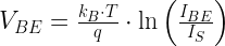
Equation 2 shows us that simply subtracting the VBE values at two different current levels will give us a value that varies directly with absolute temperature (°K). But we cannot measure VBE directly because we have losses in the wire. How do we deal with those?

Wire Losses

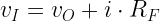
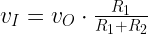
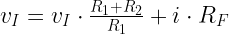
Figure 2 shows the the model I will use for analyzing how Woodward drives the sensor. Note that I have lumped all the wire resistance into a single variable RLoss.

Figure 2: Wire and Sensor Model.

Figure 2: Wire and Sensor Model.

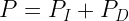
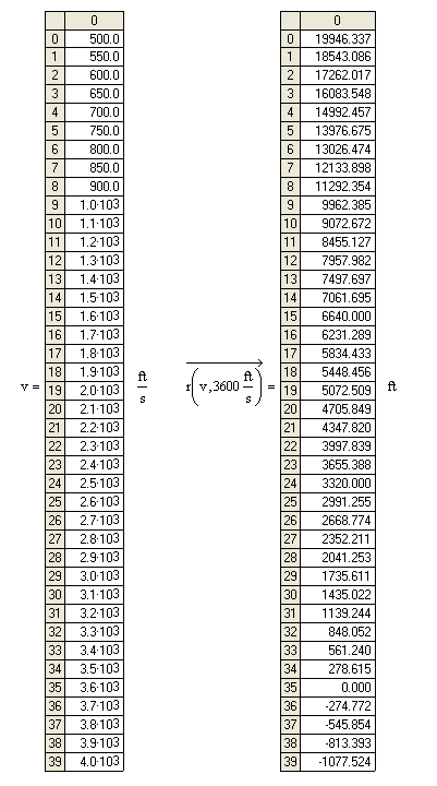
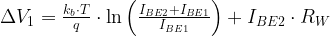
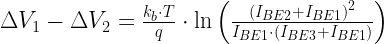
In Equation 3, I define two variables, ΔV1 and ΔV2. ΔV1 is the difference in VLine when the stimulus is IBE = IBE2 +IBE1 and IBE = IBE1. Similarly, ΔV2 is the difference in VLine when the stimulus is IBE = IBE3 +IBE1 and IBE = IBE1. Woodward also sets IBE3=2IBE2. Woodward uses an operational amplifier hooked up as a differential amplifier to create an output voltage equal to 2ΔV1 -ΔV2. As is shown in Equation 3, this linear combination eliminates the terms due to wire loss! We now have an output voltage that varies linearly with absolute temperature (°K).

Eq. 3 \Delta {{V}_{1}}=\frac{{{k}_{b}}\cdot T}{q}\cdot \ln \left( \frac{{{I}_{BE2}}+{{I}_{BE1}}}{{{I}_{BE1}}} \right)+{{I}_{BE2}}\cdot {{R}_{W}}
\Delta{{V}_{2}}=\frac{{{k}_{b}}\cdot T}{q}\cdot \ln \left( \frac{{{I}_{BE3}}+{{I}_{BE1}}}{{{I}_{BE1}}} \right)+{{I}_{BE3}}\cdot {{R}_{W}}
\Delta{{V}_{2}}=\frac{{{k}_{b}}\cdot T}{q}\cdot \ln \left( \frac{2\cdot {{I}_{BE2}}+{{I}_{BE1}}}{{{I}_{BE1}}} \right)+2\cdot {{I}_{BE2}}\cdot {{R}_{W}}
\Delta {{V}_{1}}-\Delta {{V}_{2}}=\frac{{{k}_{b}}\cdot T}{q}\cdot \ln \left( \frac{{{\left( {{I}_{BE2}}+{{I}_{BE1}} \right)}^{2}}}{{{I}_{BE1}}\cdot \left( {{I}_{BE3}}+{{I}_{BE1}} \right)} \right)

Unfortunately, Equation 3 has a non-zero value at 0 °C because T is expressed in absolute temperature (°K). We now need to make this output voltage vary linearly with Celsius temperature (°C).

Linear Variation with °C

The final bit of analog signal processing is fairly straightforward. We have three things to do:

  • Generate the linear combination 2ΔV1(T) -ΔV2(T).
    This computation eliminates voltage loss other than from the transistor BE junction.
  • Shift this curve down by the value of 2ΔV1(273.15 °K) -ΔV2(273.15 °K).
    273.15 °K is the same as 0 °C. This makes our output voltage equal to 0 V when T = 0 °C.
  • Apply gain to the circuit to scale the output so that 0 °C to 100 °C is represented by 0 V to 10 V.
    The voltage range of 0 V to 10 V is arbitrary, but is easy to measure accurately. Figure 3 shows a simplified version of Woodward's output circuit.
Figure 3: Output Amplifier Circuit.

Figure 3: Output Amplifier Circuit.

We need to compute some resistor values for this circuit. I will use Mathcad for this part of the exercise. First let's define some terms and functions (Figure 4).

Figure 4: Definitions for Computational Work.

Figure 4: Definitions for Computational Work.

We now need to derive an expression for the output voltage from the op-amp in terms of resistors (Figure 5). Note that some expression were long and are chopped in Figure 5. That happens sometimes.

Figure 5: Solve for the Op-Amp Output Voltage.

Figure 5: Solve for the Op-Amp Output Voltage.

These resistor values work for the circuit of Figure 3, but VOffset is a small value that is difficult to generate directly. Woodward used a Thevenin equivalent circuit to generate the offset voltage and required input resistance. I compute these values in Figure 6.

Figure 6: Thevenin Equivalent Circuit for Generating the Offset Voltage.

Figure 6: Thevenin Equivalent Circuit for Generating the Offset Voltage.

All resistances are now determined. The capacitor values are not particularly critical and I will not go into detail as to how they are selected.

Circuit Sequencing

The circuit is a bit confusing until you see that it uses a two-bit counter to cycle through the stimulus current values (see Figure 7). This counter applies currents to the transistor sensor in the order I1, I1+I2, I1, I1+I3. If you look at the circuit carefully, you will see that Woodward is using the multiplexer to charge the 1 μF capacitors with the proper polarities so that their sums generate ΔV1 and ΔV2. It is a little tricky, but just look at Figure 7 carefully and you will see how he does it.

Schematic

I have included the schematic for reference in Figure 7 (Source).

Figure 7: Woodward Schematic.

Figure 7: Woodward Schematic.

Conclusion

This circuit is very representative of Woodward's work. His circuits are fine examples of applying component physics in an economical fashion to real-world applications. I will have a few more posts that cover some of his other work.

Posted in Electronics | Comments Off on An Analog Circuit Design Review