Rigging Cables is Really Important

Quote of the Day

History is a tool used by politicians to justify their intentions.

— Ted Koppel


I have been rather frustrated lately with the number of field failures I have encountered that are related to the humble cable tie (Figure 1 - Source).

Figure 1: Assortment of Cable Ties.

Figure 1: Assortment of Cable Ties.

There are several problems related to cable ties.

  • They are easy to over-tighten

    Many people tighten the cable ties so tightly that the damage the insulation of the wires.

  • If your cables move, the cable ties tend to "bite" into the insulation.

    I just encountered this problem in our office. Instead of standard whiteboards for marking, we use SMART boards. One of our SMART boards behaved very erratically. As we investigated, we discovered that the cable tie used to secure a cable had abraded the insulation off of some wiring.

  • They can be used to tie cables in positions that put strain on connectors.

    This problem has created some real problems for me. The cable riggers pulled that cables at very odd angles which put strains on Printed Circuit Boards (PCBs). PCBs are not designed to be under mechanical strains and we have seen issues.

I started to look around for good examples of cable rigging that did not use cable ties. I soon found that the folks at NASA have done some very nice rigging on their Mars rovers. Figure 2 shows one example. For a great discussion of rigging for Mars, see this forum discussion.

It is not hard to believe that NASA understands cable rigging. They have had some issues in the past and they learn from their mistakes (e.g. Space Shuttle and Apollo 1).

Figure 2: Mars Curiousity Rover Cable Rigging.

Figure 2: Mars Curiosity Rover Cable Rigging.

I have found some good aerospace reference material on rigging that I want to make more readily available. These methods seem very reasonable to me.

I will be using these standards in my engineering group for guidance. There are a number of vendors that put out rigging supplies. Here is one vendor recommended in the forum of Guild of Knot Tyers.

There is also some good material put out by the telecommunications companies -- some of this material is over 100 years old (Old 50 MByte Telephone Spec). For example, Figure 3 shows an approach from this old material that I still occasionally use.

Figure 3: I Often Use This Approach to Cleaning Finish the End of A Cable.

Figure 3: I Often Use This Approach to Cleaning Finish the End of A Cable.

In the old days, they even referred to sewing cables together (Figure 4).

Figure 4: Example of Cable Sewing.

Figure 4: Example of Cable Sewing.

On a personal note, I am a big knot person. Studying knots and their application have been a recreational activity of mine for years.

Save

Posted in Electronics, Personal | 6 Comments

Example of Error Calibration

Quote of the Day

I am not a product of my circumstances. I am a product of my decisions.

— Stephen Covey


Introduction

I was reviewing a test report today for an optical receiver with an integrated power measurement sensor. This sensor is not particularly accurate -- its accuracy was specified as within ± 3 dB of true. This is not good at all. As I looked at our test data, I immediately noticed that I could calibrate the sensor to get a much more accurate result. But as I continued to think about the problem, I decided not to calibrate the sensor. The decision was driven by the cost of calibration versus the value of a more accurate result to the customer. Let's look at how I made this decision -- no magic here -- just a common engineering tradeoff.

Background

Some Definitions

The Wikipedia has reasonable definitions for sensors and transducers.

Sensor
A sensor is a converter that measures a physical quantity and converts it into a signal which can be read by an observer or by an instrument.
Transducer
A transducer is a device that converts a signal in one form of energy to another form of energy. Energy types include (but are not limited to) electrical, mechanical, electromagnetic (including light), chemical, acoustic and thermal energy. While the term transducer commonly implies the use of a sensor/detector, any device which converts energy can be considered a transducer. Thus, a motor is a transducer.

I should also spend a bit of time discussion my views on calibration versus compensation.

Calibration
According to the Wikipedia, calibration is a comparison between measurements – one of known magnitude or correctness made or set with one device and another measurement made in as similar a way as possible with a second device. I view calibration as a measurement process designed to generate mathematical parameters needed to adjust a transducer's real output closer to some idealized value.
Compensation
According to the Wikipedia, compensation is a plan to mitigate the effect of expected side-effects or imperfections. I view compensation as the procedure that uses calibration data to "correct" the output of a transducer.

Sensor Errors

By the definitions given above, a sensor converts a physical quantity that cannot be directly measured into a form that can be directly measured. Unfortunately, all conversions are at some level imperfect. As long as the conversion errors do not vary with time, we can use simple table or polynomial-based error compensation approaches.

The degree of error compensation you require often drives the compensation approach you use. I remember talking to an engineer who was trying to measure temperature to a tiny fraction of a degree. His solved his problem using very  time-consuming, high-accuracy temperature measurements and an assortment of piecewise, seventh-order polynomials to compensate for the errors in his sensors. My accuracy requirements are not so severe. I would like to be able to measure optical power from -10 dBm to -30 dBm with an accuracy of ±0.5 dBm.

In the case I will be discussing here, I have a sensor with a digital interface (i.e. there is a processor with an I2C interface embedded in the sensor) that will tell me the optical power present on a fiber. Ideally, if I have -20 dBm of optical fiber on the fiber, my sensor will tell me that I have -20 dBm on the fiber. If my sensor with digital interface were ideal, I would have an optical power measured versus actual optical power that is linear  with slope 1 and intercept 0. Let's call the graph of optical power measured versus actual optical power my sensor's response curve.

Unfortunately, the digital value returned by the sensor and its interface are only specified by the vendor as accurate within ±3 dB. However, the sensor response is fairly linear -- the only problem is that the sensor plot has a slope that is not 1 and an intercept that is not 0 . This means that we can model the error using two parameters:

  • gain error

    This term represents the slope error (i.e. deviation from 1)  in my sensor's response curve.

  • bias error

    This term represents the intercept error (i.e. deviation from 0) of my sensor's response curve.

Role of Calibration

When a sensor has a processor embedded with it, you could calibrate the sensor to minimize the reported error. In my situation here, the sensor appears to have a linear characteristic that could be corrected well by a simple linear transform. However, the sensor vendor chose not do that. Why?

I am pretty sure I know why -- they did not want to spend the money to calibrate the sensor. Calibration of an analog sensor can be costly because:

  • You need certified source (i.e. optical power in this case) to stimulate the sensor.
  • You need to re-qualify your test fixture periodically.
  • It is expensive to build a repeatable, certifiable test fixture.
  • You need to pay for test time.

However, you only need to pay this money if you want the accuracy. In my case, this sensor vendor made their sensor less expensive by not calibrating it. If I want more accuracy, I would need to calibrate it myself. Now I need to decide if the cost of calibration is worth it.

Analysis

I spent some time looking at the sensor. Here are my results.

Raw Sensor Data

Figure 1 shows the actual sensor response (i.e. power in versus measured power). Observe that the characteristic is quite linear over the -10 dBm to -30 dBm range that I am interested in. However, the line does not have a slope of 1 nor an intercept of 0.

Figure 1: Raw Sensor Data Versus Input Data.

Figure 1: Raw Sensor Data Versus Input Data.

Compensated Sensor Data

Figure 2 shows the compensation approach. The compensation is based on the best-fit slope and intercept values measured in Figure 1.

Figure 2: Simple Compensation Approach Using Linear Model (Gain and Bias Error).

Figure 2: Simple Compensation Approach Using Linear Model (Gain and Bias Error).

Figure 3 shows my compensated sensor reading versus the actual optical power. Simple linear compensation looks very effective.

Figure 2: Compensated Sensor Data.

Figure 3: Compensated Sensor Data.

Conclusion

By spending money on calibration, I can reduce my optical power error from ±3 dBm to ±0.5 dBm. The cost was a ~1 minute of tester time, which means ~$2 per unit. While I prefer to have more accuracy, does it really matter to a customer? How will they use this information?

  • They will use the power data to ensure that their received optical power is within the dynamic range of their receivers

    Most customers (~95%) run their networks in the middle of the dynamic range of the system. Since we have 15 dB of dynamic range, ±3 dBm of inaccuracy is not important to most customers. Do we want to burden everyone with the expense of performance needed by a few -- probably not.

  • They will use the power data to determine if any of their optical components are aging.

    In this case, accuracy is not so important as precision. The customers will simply track how their optical power levels move with time. As long as the measurements are repeatable, they really do not need to be that accurate.

So I have decided not to calibrate the sensor. The uncalibrated sensor is accurate enough for 95% of the customer base. For that 5% that need an accurate sensor, we will need to provide them with an off-the-shelf test equipment option. However, the bulk of our customers will not need to pay for the extra accuracy.

Posted in Electronics | Comments Off on Example of Error Calibration

Tire Pressure Math

Quote of the Day

Courage is what it takes to stand up and speak; courage is also what it takes to sit down and listen.

— Sir Winston Churchill


Introduction

I woke up this morning to a rather brisk temperature of -23 °F (-31 °C). This is cold. At work, we had a short hallway discussion on the impact of temperature on tire pressure. I mentioned the following "rule of thumb" for tire pressure versus temperature (one of many sources):

Tire pressure decreases by 1 psi for each 10 °F decrease temperature.

This rule of thumb is easily derived and I thought I would put out a quick post on the subject. According to this rule, my tire pressure has dropped 6 psi since I filled my tires last week. The rule as stated assumes a nominal tire pressure of ~40 psi. You will see the rule changed to 2 psi for 10 °F of temperature change for a commercial truck tire, which are often inflated to 80 psi or more. As you will see below, the nominal tire pressure affects the amount of pressure variation with temperature.

Background

My derivation will be based on the ideal gas law. I will also make the following assumptions:

  • The ideal gas law is valid for air under pressure.

    The ideal gas law works well for low-pressure gases and gas mixtures, but it becomes less accurate as pressures increase. It turns out that at typical tire pressures, the error is less than 1% (see Appendix A).

  • The volume of the tire changes insignificantly with pressure.

    Tires are pretty stiff (e.g. they may have Kevlar or steel cords embedded in them). I know that severe under-inflation is obvious because the tire material is sagging. However, tires near full inflation vary little in volume as pressure changes.

Analysis

General Result

Given the assumptions above, we can derive an expression that states that the percentage change of air pressure in a tire is inversely proportional to the tire air temperature (Equation 1).

Eq. 1 \Delta p\%\triangleq \frac{\frac{dp}{dT}}{p(T)}=\frac{1}{T}

where

  • T is the absolute temperature of the tire air.
  • p(T) is the tire air pressure as a function of temperature.
  • \Delta p\% is the percentage tire pressure change with temperature.

We can derive Equation 1 as shown in Figure 1.

Figure 1: Derivation of Equation 1.

Figure 1: Derivation of Equation 1.

Ideal Gas Law Universal Gas Constant

Specific Example

Figure 2 shows how we can apply Equation 1 to a common tire pressure scenario to give us the rule of thumb. The tire pressure scenario is:

  • Tire air temperature of 20 °C (68 °F).
  • Sea level air pressure of 14. 7 psi.
  • Nominal tire pressure of 40 psi (gauge pressure)

I should note that Mathcad automatically converts the temperatures to an absolute scale (e.g. Kelvin). So when you see an expression like "(-20)°F", understand that this temperature is being converted into Kelvin.

Figure 2: Derivation of the Rule of Thumb for a Tire Pressure of 40 psi.

Figure 2: Derivation of the Rule of Thumb for a Tire Pressure of 40 psi.

We see in the example that the change in tire pressure with temperature is about 1 psi for every 10 °F change in temperature for a 40 psi tire pressure at 68 °F. In Figure 2, I look at two different air temperatures. You will notice that for a given tire pressure, the pressure change with temperature increases with lower reference temperature.

Figure 3 shows a graph of how the tire pressure (40 psi @ 68 °C) varies with temperature.

Figure 3: Tire Pressure Graph.

Figure 3: Tire Pressure Graph.

Conclusion

Straightforward application of the ideal gas law. Pretty simple post.

Appendix A: Compressibility Factor for Air

The compressibility factor for air is shown in Table 1 (Source). The compressibility factor is the ratio of the molar volume of a gas to the molar volume of an ideal gas at the same temperature and pressure. The compressibility factor can be used as a correction factor for the ideal gas law when applied to real gases.

As you can see from the table, the compressibility factor deviates from 1 by a fraction of a one percent even at 60 psi (~5 bar absolute). This means that using the ideal gas law will result in an error of less than 1%.

Table 1 : Air Compressibility Factor Table.

Pressure,
bar (absolute)

Temp,
K

1

5

10

20

40

60

80

75

0.0052

0.0260

0.0519

0.1036

0.2063

0.3082

0.4094

80

0.0250

0.0499

0.0995

0.1981

0.2958

0.3927

90

0.9764

0.0236

0.0453

0.0940

0.1866

0.2781

0.3686

100

0.9797

0.8872

0.0453

0.0900

0.1782

0.2635

0.3498

120

0.9880

0.9373

0.8860

0.6730

0.1778

0.2557

0.3371

140

0.9927

0.9614

0.9205

0.8297

0.5856

0.3313

0.3737

160

0.9951

0.9748

0.9489

0.8954

0.7803

0.6603

0.5696

180

0.9967

0.9832

0.9660

0.9314

0.8625

0.7977

0.7432

200

0.9978

0.9886

0.9767

0.9539

0.9100

0.8701

0.8374

250

0.9992

0.9957

0.9911

0.9822

0.9671

0.9549

0.9463

300

0.9999

0.9987

0.9974

0.9950

0.9917

0.9901

0.9903

350

1.0000

1.0002

1.0004

1.0014

1.0038

1.0075

1.0121

400

1.0002

1.0012

1.0025

1.0046

1.0100

1.0159

1.0229

450

1.0003

1.0016

1.0034

1.0063

1.0133

1.0210

1.0287

500

1.0003

1.0020

1.0034

1.0074

1.0151

1.0234

1.0323

600

1.0004

1.0022

1.0039

1.0081

1.0164

1.0253

1.0340

800

1.0004

1.0020

1.0038

1.0077

1.0157

1.0240

1.0321

1000

1.0004

1.0018

1.0037

1.0068

1.0142

1.0215

1.0290

Posted in General Mathematics, General Science | 10 Comments

A PCB Thermal Computation Example

Quote of the Day

The creation of a thousand forests is in one acorn.

— Ralph Waldo Emerson


Introduction

Figure 1: Apex SA57 Evaluation Printed Circuit Board.

Figure 1: Apex SA57 Evaluation Printed Circuit Board.

I am doing some self-training on electronic thermal analysis. As part of my self-training ritual, I often work through vendor application notes. This post will show how I work through an application note using Mathcad. I chose the Apex SA57 evaluation board (Figure 1) because Apex had the most complete worked example that I have seen.

You might think that there is nothing special about working through someone else's calculations, but this particular exercise shows how things do not always go smoothly. I frequently find errors in vendor application notes. This application note was no exception, and I worked with the vendor to correct it. They appreciated the in-depth review and are now in the process of correcting their documentation.

For those interested in the fine details, my Mathcad source and its PDF are here.

Background

Goals

I am always looking at new electronic parts. This blog post is about working through an application note for estimating the thermal resistance of a power Integrated Circuit (IC) on a two-layer Printed Circuit Board (PCB). Since I am just learning about thermal analysis, this will be a learning experience for me.

As one of my physics professors used to tell me, "You cannot say you understand the material until you can work the problems." To make sure that I can correctly apply new knowledge, I work through some of the application examples that the electronic part vendors put together. If I can duplicate their results, then I feel that I am ready to begin working on my problems.

Approach

As part of my self-education, I need to organize my work. There are three tools I use in this effort:

  • Mathcad

    All of my learning involves mathematics. I NEVER do mathematics manually. I always create Mathcad worksheets to document my calculation efforts.

  • Note Taking Tool

    I use a tool called Whizfolders. I also know folks who use OneNotes. It is a matter of personal preference. Religiously using a note-taking tool ensures that you never lose information. It also greatly speeds your access to information years later.

  • Excel

    I use Excel for routine data management. I like its editor and I use it to beat data into forms convenient for analysis.

With my tools in place, it is now time time to dig into the application note. Here is a link to the original application note I found on the web. Because things move around on the web, I have included a copy on my personal web site. As I mentioned, I found some issues and the vendor gladly agreed to correct their note. Their corrected note has not been issued yet, so I have included a corrected version of the note here. My corrections are in red and they have been confirmed by the part vendor, Apex Microtechnology.

You may have noticed that I am detail-oriented – I always tell people that my career has been a celebration of detail …

Key Technical Points

Basic Thermal Resistance Equation

Equation 1 shows the formula for thermal resistance that I will be applying repeatedly in the following analysis.

Eq. 1 \displaystyle {{R}_{X}}={{\rho }_{X}}\cdot \frac{{{l}_{X}}}{{{A}_{X}}}=\left( \frac{1}{{{\lambda }_{X}}} \right)\cdot \frac{{{l}_{X}}}{{{A}_{X}}}

where

  • λX is the thermal conductivity of the material that makes up object X (Reference).
  • ρX is the thermal resistivity of the material that makes up object X \left( {{\rho }_{X}}\triangleq \frac{1}{{{\lambda }_{X}}} \right).
  • lX is the length of object X along the path of conduction.
  • AX is the area of object X along the path of conduction.
  • RX is thermal resistance of object X.

Overall Thermal Model

Figure 2 shows a cross-section of the power IC I am looking at using and how it is mounted to a PCB.

Figure 1: Apex Power IC Mounting on a PCB.

Figure 2: Apex Power IC Mounting on a PCB.

The power from the integrated circuit moves from the silicon to the bottom of the circuit board. We assume the bottom of the PCB is an isothermal (i.e. constant temperature) region – on the real card, this means that the bottom-side heat sink (Figure 1) couples the bottom of the card to the ambient air perfectly (i.e. no thermal resistance). Obviously, this is an idealization but one that a more sophisticated model can easily include.

Figure 3 shows how they model the configuration of Figure 1 using thermal resistances.

Figure 2: Thermal Model Used in the Apex Application Note.

Figure 3: Thermal Model Used in the Apex Application Note.

Thickness of Copper Planes

Figure 4 shows how we can compute the thickness of the copper foil used in the PCB to construct the copper traces, regions, and layers. The thickness of copper foil is usually specified in terms of the weight of one square foot of the copper foil.

Figure 4: Formula for Thickness of Copper Foil Based on Mass.

Figure 4: Formula for Thickness of Copper Foil Based on Mass.

Copper Information

The application note computes each of the individual thermal resistances and a total thermal resistance. I will duplicate this work.

Analysis

Key Thermal Constants

Figure 5 shows some of the constants used in the analysis to follow.

Figure 4: Key Thermal Constants.

Figure 5: Key Thermal Constants.

Silicon Information Copper Information FR4 Information Aluminum Information

Thermal Resistance of the Silicon Die

The transistors on the IC dissipate power. Integrated circuits place their power dissipating elements on one side of a slab of silicon. This power must pass through the silicon to an aluminum slug, which conducts the heat from the silicon to the top of the PCB. Figure 6 shows the calculations.

Figure 5: Thermal Resistance of the Silicon Die.

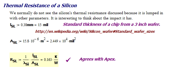
Figure 6: Thermal Resistance of the Silicon Die.

Silicon Thermal Resistance

Thermal Resistance of the IC's Heat Slug

Figure 7 shows the calculations for the thermal resistance of the heat slug.

Figure 6: Thermal Resistance of the Heat Slug.

Figure 7: Thermal Resistance of the Heat Slug.

Thermal Resistance of the Copper Pad on Top PCB Layer

Figure 8 shows the calculations of the copper pad on the top of the PCB. The IC's heat slug sits on this copper pad.

Figure 7: Thermal Resistance of the Copper Pad on Top of the PCB.

Figure 8: Thermal Resistance of the Copper Pad on Top of the PCB.

Thermal Resistance of the PCB

The PCB thermal model is a composite of vias, laminate, and planes. I break this modeling down in the following subsections.

Thermal Resistance of the FR4 PCB Material

Figure 9 shows how I calculated the thermal resistance of the FR4 PCB material.

Figure 8: Thermal Resistance of FR4 Material in the PCB.

Figure 9: Thermal Resistance of FR4 Material in the PCB.

Thermal Resistance of a 20 mil Via

Figure 10 shows the calculations for the thermal resistance of a 20 mil via.

Figure 9: Formula for the Thermal Resistance of a Via.

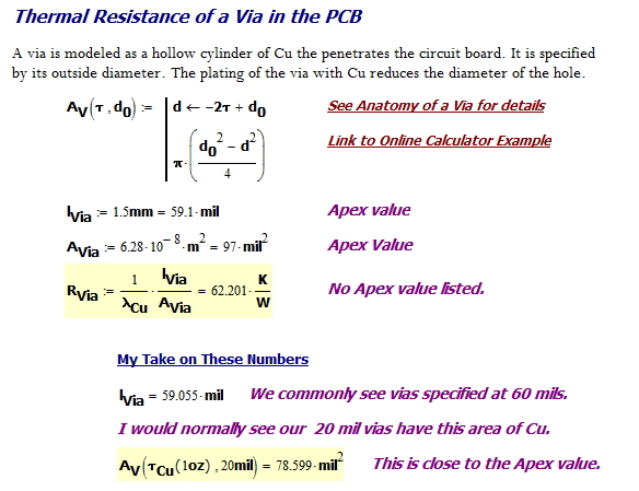
Figure 10: Formula for the Thermal Resistance of a Via.

anatomy of a plated through hole Online via thermal resistance calculator

Thermal Resistance of the PCB with 24 Vias

Figure 11 show the calculations for the thermal resistance of the overall PCB (i.e. FR4 material thermally in parallel with 24 vias). Observe that the vias have a combined thermal resistance of ~2.6 Ω, which is modeled as a parallel resistance to laminate's thermal resistance of ~58 Ω. Clearly, most of the heat moves through the vias.

Figure 11: Thermal Resistance of the Overall PCB.

Figure 11: Thermal Resistance of the Overall PCB.

Thermal Resistance of the PCB Bottom Copper Layer

Figure 12 shows how the thermal layer of the PCB's bottom copper layer is computed.

Figure 10: Thermal Resistance of the Bottom Copper Layer on the PCB.

Figure 12: Thermal Resistance of the Bottom Copper Layer on the PCB.

Overall Thermal Resistance Calculation

Figure 13 shows the overall thermal resistance calculation. Observe that nearly 85% of the thermal resistance is in the PCB – without vias, this percentage and RTotal would have been much larger.

Figure 13: Total Thermal Resistance Calculation.

Figure 13: Total Thermal Resistance Calculation.

Conclusion

This was a good computation exercise. Let's review the results:

  • This exercise presented a good example of a power-focused, analog design.
    • This example used a heat sink – most digital designs do not include heat sinks.
    • In applications without fans, getting the heat to the air is a big challenge.
  • All the calculations were based on Equation 1, which is analogous to the formula for the resistance of an electrical conductor.
  • The thermal resistance of the PCB dominates the overall thermal resistance
    • Adding more copper to the PCB can help (e.g. 2 oz Cu planes), but this will make the PCB more difficult to solder and rework.
    • The role of the via to the overall PCB thermal resistance is critical.
    • You need to place as many vias as you can between the top and bottom layers.
    • For high -power circuit boards, you may wish to use other laminate materials – their thermal resistance varies quite a bit
      • {{\lambda }_{{FR4}}}=0.26\frac{W}{{m\cdot K}}
      • {{\lambda }_{{RO4003C}}}=0.71\cdot \frac{W}{{m\cdot K}}
    • FR4 is the cheapest laminate you can find. Any others will cost more.

Save

Save

Save

Save

Save

Save

Save

Posted in Electronics | 6 Comments

Wasted School Time

Quote of the Day

Censorship reflects a society's lack of confidence in itself.

- Potter Stewart


Introduction

I frequently talk to young engineers who have just completed university. I am always curious as to what they studied in school. I sometimes wonder how much of their education time will end up having been wasted. I completely understand that each school has a set curriculum that they must follow in order to make sure that all of their students are receiving a well-rounded education. It is their job to do this. And don't get me wrong, they do it well, especially if you have found that you rank high on the school league tables for the type of educational establishment that you run due to grades and other findings. It's great, and it's definitely an achievement worth celebrating.

While there are many students who value school and think that it is the best years of their life because of what they have learned, you'd be surprised to know that there are others who feel that their school life has been wasted. I'm yet to clarify just how much of this time they are talking about. I ask that question because so much of my education time was spent on things that ended up being of no use or just plain wrong -- particularly in junior high and high school.

Let me give you a few examples. The list is far from complete, but you will get my point.

Grade School Wastes of Time

  • Cursive Writing
    I have never cursively written more than my signature in my entire life.
  • Every class emphasized that the US needs to win the Vietnam War.
    The Vietnam War was equated with making the world safe for democracy. This was beat on very hard in 5th and 6th grade. Lots of discussion about dominoes, but they never told us what a domino was. I had to ask my father, who played dominoes when he was in the US Army. You could tell that the Tet Offensive in 1968 put doubt into many people's minds.
  • Lots of discussions on communism versus capitalism.
    This discussion is probably left to history classes today.
  • Characteristics of fallout
    My staff and I have been sharing stories of all the stuff they taught us about fallout. Things like:

    • Don't drink milk because it might contain strontium-90 (I still remember this isotope).
    • You can wash most of the fallout off, just make sure you don't breath it in.
    • Half-life ... this is where I learned about half-life.
  • How to build a fallout shelter.
    A government representative handed me a green and white pamphlet that showed how my family could build different kinds of fallout shelters, which I read very carefully. After I completed studying the pamphlet, I told my father that building a shelter was going to be a lot of work and we should start on it right away. My father said don't worry about it -- we lived near Minneapolis (a major population center) and had no hope of surviving a nuclear attack. His answer bothered me, but he was right.
  • A huge amount of time spent on the evils of marijuana.
    The training emphasized marijuana as a gateway drug that led right to heroin. I used to live in Colorado -- they have now legalized marijuana.
  • Endless hours in religious education.
    None of it worked on me. As my mother says, I am hopeless. In an effort to give me a bit more religious focus, we tried one year in Catholic school. That is the year my mother and I agree not to discuss anymore.

Junior High School Wastes of Time

I went to a school that focused on vocational training. Most of this training was obsolete by the time I left university.

  • Logarithm and trig function tables (including linear and quadratic interpolation)
    I have never used these tables for a real problem.
  • Hand drafting
    In real life, I have only done CAD.
  • Offset Printing
    Anybody done any offset printing lately?
  • Learning the California Job Case
    We had to memorize the placement of steel type in a wood chest. Anybody set any type lately?
  • Film development
    I don't think I need to say any more.
  • Using typewriters and mimeograph machines
    I haven't used any of these outside of school either.
  • Anti-smoking education
    I watched cigarettes kill my father -- I never once considered smoking.
  • How to work with video tape and film strips.
    Pretty much dead technologies.
  • Social Studies classes telling us that we were winning the Vietnam War
    Our school pushed the importance of going into the military pretty hard. They even had a colonel and sergeant come into our one of our history classes to tell us that the Vietnam War was really going very well and draft dodgers should just stay in Canada. They implied the media was lying to us.

High School Wastes of Time

As with my junior high school, my high school had a strong focus on vocational education.

  • Taking a deviant social behavior class
    If I told you what was considered a deviant social behavior in the early 1970s in rural Minnesota, you wouldn't believe it – or maybe you would. Today, everything we discussed in this class is now a lifestyle option.
  • Punch cards
  • All my interactions with career counselors.
    They kept giving me tests that told them I needed to become a carpenter, a field which I never wanted to do for a living. I wanted to become an engineer, but none of the counselors knew what an engineer was and they were no help in guiding me toward an engineering career.
  • Learning how to rebuild carburetors.
    I have not seen a carburetor in a long time.
  • My social studies classes that emphasized that we can now see the light at the end of the Vietnam War tunnel.
    I guess they were right about the war ending soon, just not the way they thought it would. This particular installment of my Vietnam War indoctrination ended with the warning that we needed to register for the draft. I ended up being too young to go. However, I did get a draft card.

University Wastes of Time

My university training was actually pretty focused and there were relatively few wastes of time. Since I was training to be an engineer, the items are all technological.

  • Training on the slide rule
    I still have my old slide rule -- I couldn't tell you how to use it. I had several professors tell me not to use those newly introduced calculators because you lose your feel for numbers. Today, I NEVER manually do any arithmetic. It would be embarrassing for people to see how bad I am at manual arithmetic. I do not worry about it.
  • Booting my computer with paper tape.
    Ahh ... the old PDP-8 ... memories ...
  • Using Teledeltos paper
  • Using rubylith
  • How to use a nomograph.
    I actually think nomographs are interesting, but they have been of no use in my daily work.
  • Learning about magnetic bubble memory.
  • Learning about NMOS IC design.
    CMOS replaced it right after I learned how to design chips with NMOS.
  • Learning about MSI TTL design.
    I moved from custom chips to ASICs to FPGAs. I was not really a medium-scale integration person.

A Story of Wrong Choices

We all have to make education choices and those choices often do not look wise when viewed from a later date. I was taking a training course (in transputers -- another dead technology) at the University of Rochester. While there, I had lunch with a physics professor who had education stories similar to mine. Here is one of his tales.

I had just completed my undergraduate degree and I needed to find a physics professor with a research program that was going to get me into a high-paying startup company. The first professor I interviewed was working on something called "liquid crystals" and he said that someday that technology would be used to make cheap, low-power displays. I thought he was nuts, so I moved on. [Today, liquid crystal displays are a multi-billion dollar market]

I interviewed another professor who was doing work on making semiconductor lasers. I couldn't see where there would be any market for this technology. I thought he was nuts. [Today, semiconductor lasers are used everything from DVD players to high-speed fiber optic communications]

I then interviewed a professor who was working on magnetic bubble memory. Now there was a technology that was going to go places. [Today, bubble memory is considered a historical oddity -- it went nowhere]

Like any investment, education has its risks -- sometimes it pays and sometimes it doesn't.

Posted in Osseo, Personal | 4 Comments

Times of Latest Sunrise and Earliest Sunset

Quote of the Day

The road to wisdom? Well, it's plain and simple to express. Err and err and err again, but less and less and less.

— Piet Hein


Introduction

I have lived most of my life in Minnesota, so you would think that I would be used to cold weather by now. The key to having a pleasant winter is dressing properly. The one thing that I still struggle with is the short duration of our daylight in winter. Because of our limited daylight, I need to know the time of sunrise and sunset to plan my outdoor activities. So every morning I listen to the radio when they list our local  sunrise and sunset times.

I recently noticed that the date of our earliest sunset was coming six days before the winter solstice. I then checked the date of our latest sunrise and that date was twelve days after the winter solstice. I know that the winter solstice has the shortest daylight duration of all the days of the year, but it has neither the latest sunrise nor the earliest sunset. This seemed odd to me. Let's investigate these observations.

Background

Scope

I will be focusing my discussion on Minneapolis, which is the largest city near my home. I obtained my sunrise, sunset, and daylight duration times for Minneapolis from this web site.

I will not derive the formulas used to compute sunrise and sunset times as these formulas are well document elsewhere (e.g. formula for both). For this post, I chose to obtain my data from a web page (I am getting lazy in my old age).

Definitions

The terms sunrise and sunset are defined in terms of the Sun's position relative to the horizon. The fact that things start getting dark as the Sun rises and sets  is associated with atmospheric light scattering. We use terms like dusk and twilight. to describe the light level present.  Figure 1 illustrates the Sun's position relative to the horizon  for the terms sunrise, sunset, dusk, dawn, and twilight (Source).

Figure 1: Illustration of the Terms Sunrise, Sunset, Horizon, and Twilight.

Figure 1: Illustration of the Terms Sunrise, Sunset, Dusk, Dawn, Horizon, and Twilight.

My analysis will be focusing on sunrise and sunset time.

Analysis

Approach

I just grabbed the sunrise, sunset, and daylight duration numbers for Minneapolis from this web page and plotted them in Excel.

Daylight Duration

Figure 2 confirms that the winter solstice (Dec 21 in 2013) has the shortest daylight duration.

Figure 2: Daylight Duration Around the Winter Solstice.

Figure 2: Daylight Duration Around the Winter Solstice.

Sunrise and Sunset Times

Figure 3 shows the sunrise and sunset times around the time of the winter solstice. Notice how the earliest sunset occurs six days before the winter solstice, and the latest sunrise occurs twelve days after the winter solstice.

Figure 3: Times of Latest Sunrise and Earliest Sunset in Minneapolis.

Figure 3: Times of Latest Sunrise and Earliest Sunset in Minneapolis.

While the time of earliest sunset occurs six days before the winter solstice, our days continue to get shorter because the sunrise time is getting later faster than the sunset time is getting earlier. After the winter solstice, the duration of daylight begins to increase sunset time is getting later faster than the sunrise time is getting earlier.

Conclusion

Here is what I accomplished with this exercise:

  • I confirmed that the day of shortest daylight duration is the winter solstice.

    The interesting thing about this fact is that the winter solstice has neither the latest sunrise nor the earliest sunset.

  • I see that the date of earliest sunset is six days before the winter solstice.

    Sunset times are later for the six days after Dec 15th. You would think that later sunsets means more total daylight, but sunrise is coming so late as to more than compensate for the later sunset.

  • I see that the date of latest sunrise occurs twelve days after the winter solstice.

    At this point, we now start seeing the duration of daylight begin to increase more rapidly.

Posted in Astronomy, General Science | 3 Comments

Benjamin Franklin's Long Term Financial Planning

Quote of the Day

The secret of joy in work is contained in one word -- excellence. To know how to do something well is to enjoy it.

- Pearl Buck


Today, my youngest son and I were talking about different investment strategies we have heard about. We spent quite a bit of time discussing Warren Buffet's focus on durable competitive advantage and his statement about long term investing.

Life is like a snowball. The important thing is finding wet snow and a really long hill.

The same can be agreed upon for investing, truth be told. Whether it be with help (from https://www.sofi.com/investing-101-center/ or others, for instance) or if you go it alone, it is an important lesson to learn. Still, during this conversation, I mentioned that the longest-term investor that I knew of was Ben Franklin, who had a two-hundred year planning horizon for one of his investments and he didn't have an equity release company looking out for him. My son had not heard this story before and maybe some of you have not heard it.

Ben Franklin set up a financial trust for Boston and Philadelphia that would provide them benefits for a two-hundred year period. His math was spot on -- unfortunately, the cities were not always the best stewards of his money and they did not realize the full value of his investment. In spite of their poor management, his investments did end up valued at $6.5M in 1991.

Let's review how compound interest gave Ben millions of dollars to distribute long after his death. The relevant financial details are as follows:

  • Boston and Philadelphia were each bequeathed £1000.
  • The money was to be loaned to young apprentices at a 5% interest to help them setup businesses
  • After 100 years, this money would have grown to £131K in each city's account. At that time and in each city, £100K would be dispersed for public improvements. The remaining money would again be used for loans to apprenctices at 5% for another 100 years
  • After 200 years, there would be £4.07M in the accounts of each city that could be used for by the cities and their states from the public good.
  • According to this web site, £1 had a value of $4.44 in 1774 (near the time of Franklin's death in 1790).

To make sure I understand what Ben was doing, I have repeated his financial calculations in Figure 1.

Figure 1: My Verification of Franklin's Financial Calculations.

Figure 1: My Verification of Franklin's Financial Calculations.

Colonial Currency Conversion Franklin's Calculations

You can read the some of the details of his bequest at this site.

Posted in Financial | 2 Comments

Boyle's Law in the Movie "Men of Honor"

Quote of the Day

I understand that sometimes you have to win ugly, but I see no advantage in losing ugly.

— Pat Buchanan, political commentator.


I do not watch many movies and the ones I do see tend to be older. Over the Christmas holiday, I watched the movie "Men of Honor" and I noticed that Boyle's law was mentioned. Here is the Boyle's law quote from the movie:

Boyle's Law describes the behavior of gases under varying amounts of atmospheric pressure. It states that if a diver holds his breath at one hundred feet, continues holding while rising to ten feet, then the gases in his lungs increase four times. Now why is this important to a diver? Forget to exhale on the way up, and your lungs explode.

I heard the quote and I did a quick calculation in my head. It seemed like this statement was not quite correct.

After the movie, I did a more serious calculation. Figure 1 shows my work. My answer was that the lung volume will increase by a factor of three, not four. I know I am being picky, but it seems like the movie folks could get a a little detail like this correct.

Figure 1: Boyle's Law Calculations.

Figure 1: Boyle's Law Calculations.

Curious Chemical Engineer

Many thanks to the Curious ChemEng for looking at my work. I could not believe the movie got this wrong and I asked him to check me. He also suggested a plausible way they got the wrong answer.

Posted in General Science | 6 Comments

The Biggest Ball Lens I have Ever Seen

Quote of the Day

The most important thing in the world today is that England and the United States speak the same language.

— Otto Von Bismarck


We use tiny ball lenses all the time to mate our fibers up to photodetectors (Source). I was impressed when I saw a news article discussing an enormous, water-filled, ball lens being used to concentrate sunlight onto a solar array. Take a look at the Rawlemon Facebook page. I am always impressed with the green energy efforts being made in Germany. Apparently, it even generates power on overcast days.
Figure 1: Enormous Ball Lens Used for Concentrating Sunlight Onto a Solar Panel.

Figure 1: Enormous Ball Lens Used for Concentrating Sunlight Onto a Solar Panel.


There are some great graphics on this page. Here are examples:
Tracker
Comparison

Posted in Fiber Optics, General Science, optics | Comments Off on The Biggest Ball Lens I have Ever Seen

Mathcad Example Using Decibels

Quote of the Day

I learned filmmaking by studying the Old Masters - and by that I mean John Ford, John Ford and John Ford.

— Orson Welles


Introduction

I have been working on a software requirements document that involves optical power levels. I thought it might be worthwhile showing you how I use Mathcad as part of my requirements analysis process. This particular example shows how I computed the minimum optical power levels that a circuit will need detect. I used decibels for the calculations, which are not like standard "multiplicative units". Decibels are not really a unit -- they are more of a scaling. However, Mathcad handles decibels very cleanly.

Background

Decibel Basics

The Mathcad folks recommend defining special functions for doing dB and dBm conversions and that is exactly what I do. Figure 1 illustrates the definitions I used in this analysis.

Figure 1: Defining a Set of Decibel Units.

Figure 1: Defining a Set of Decibel Units.

Optical Power Basics

P0 and P1 Power Levels

Binary digital communication systems work by sending streams of bits (0s and 1s) across a communications channel. These bits have to be transferred in a form that is compatible with the channel. In the case of copper wire-based systems, we use current or voltage. In the case of fiber optic systems, we use optical power to represent the 0s and 1s. I will assume that we are using "positive logic", which means that the power used to represent a logic 1 (called P1) is higher than the power used to represent a logic (called P0). Unfortunately, measuring P0 and P1 directly requires expensive test equipment (e.g. oscilloscope with optical probe).

Because this measurement is expensive, we define two alternative parameters, average power and extinction ratio. Average power is easy to measure, which makes it the most commonly reported optical parameter. Extinction ratio is difficult to measure (i.e. also requires an oscilloscope and optical probe), but it provides us additional information as to degree of wavelength purity we will see in the laser output (i.e. smaller extinction ratio means less optical power off of our desired wavelength).

Average Power

Many inexpensive handheld instruments do a fine job of taking an average power measurement. The definition of average power is P_{Ave}=\frac{P_0+P_1}{2}, assuming that P0 and P1 are equally probable. The measurement instrumentation involved is pretty straightforward:

In most cases, the average power measurement will give us enough information to understand the condition of the fiber network (e.g. ensuring that the loss levels on the plant are within specification).

Extinction Ratio

The extinction ratio is defined as \epsilon = \frac{P_1}{P_0}. I do not know of an easy way to measure extinction ratio. It is usually measured with oscilloscope with optical probe. However, the extinction ratio is important because lasers work best with lower extinction ratios. High extinction ratios (>10) cause problems like:

  • chirp

    High extinction ratio means that charge density inside the laser's optical channel is varying greatly. This can change the effective index of refraction within the channel and will cause the laser's wavelength to change during the transmission. This is bad because a varying wavelength causes dispersion.

  • overshoot/undershoot

    High extinction ratio means that the laser is driven hard on and off. This can mean that the power level will overshoot its P1 or undershoot its P0 level. Overshooting the P1 level is bad because it be difficult for the receiver circuit to deal with the widely varying signal level. Undershooting the P0 level usually means driving the laser below threshold (i.e. the laser stop lasing). This can result in some bizarre problems, including very slow laser switching speeds.

Formulas for Translating Between (P0,P1) and (\epsilon, PAve)

Figure 2 shows how you can use the definitions for PAve and \epsilon to compute P0 and P1.

Figure 2: Deriving Equations for P1 and P2 in Terms of Extinction Ratio and Average Power.

Figure 2: Deriving Equations for P1 and P2 in Terms of Extinction Ratio and Average Power.

PON Basics

Most of my work involves Passive Optical Networks (PONs). The details of the PON are not important to understand the gist of the post. It is important to know that there are two common types of PON (I am only concerned in this example with ONT-to-OLT receive power levels):

  • B+
    • PON loss is 28 dB
    • ONT PAve= 2.5 dBm
    • ONT \epsilon= 10\text{ dB}
  • C+
    • PON loss is 32 dB
    • ONT PAve= 2.5 dBm
    • ONT \epsilon= 10\text{ dB}

Figure 3 shows the loss model I used for this post.

Figure 3: Upstream PON Power Model.

Figure 3: Upstream PON Power Model.

Analysis

B+ PON

Figure 4 shows how I calculated the 0 and 1 levels at the OLT receiver for a B+ PON.

Figure 4: Determining the Power of the "0" and "1" Levels for a B+ PON.

Figure 4: Determining the Power of the "0" and "1" Levels for a B+ PON.

C+ PON

Figure 5 shows how I calculated the 0 and 1 levels at the OLT receiver for a C+ PON.

Figure 5: Determining the Power of the “0″ and “1″ Levels for a C+ PON.

Figure 5: Determining the Power of the “0″ and “1″ Levels for a C+ PON.

Conclusion

I just wanted to show folks how I document my requirements work using Mathcad. I do this sort of analysis every day.

Save

Posted in General Mathematics, optics | 7 Comments