Outdoor Enclosure Temperature Profile Math

Introduction

We build products that mount on the outside of homes -- homes that can be anywhere in the world. This means that the temperatures can be brutally cold (e.g. -46 °C in Bemidji, MN) or brutally hot (e.g. 49 °C in Death Valley, CA). Exposure to the Sun adds to these temperatures, which we call solar load. We have been having discussions with one of our vendors about the projected reliability of their parts. This particular part is very sensitive to the total amount of time it spends above a certain temperature. Since we design our equipment to operate reliably for least 10 years under worst-case conditions, it is important for us to determine how much time this part will spend above this threshold temperature.

After some discussion, we decided to use Phoenix as our climatic reference. It is a hot place with excellent climatic data. We also have product deployed in the area that will allow us to compare our temperature profile projections with actual data. Unfortunately, I need data now and I cannot wait a year to acquire the temperature data.

In many ways, I needed a "Fermi" type answer -- order of magnitude results would have been fine. I ended up doing extensive calculations because I had no intuitive feel for the situation. However, these calculations just took a couple of hours. Complex temperature simulations would have taken weeks. I view this approach a "middle of the road" course. After shipping out the work, the following quote came to mind.

If a thing is worth doing, it's worth doing well - unless doing it well takes so long that it isn't worth doing any more. Then you just do it 'good enough' --Programming Perl, Wall and Schwartz

Background

Here is the background on the reliability of the part we are investigating in this post:

  • The part is an integrated circuit

    There is an enormous amount of data that demonstrates that integrated circuit reliability is strongly related to temperature (link to a good reference).

  • Our vendor is stating that operation above 110 °C will result in degraded operational lifetime.

    You often see 110 °C listed as a maximum junction temperature guideline. I first encountered this limit while working on government contracts where Willis Willoughby advocated 110 °C as a junction temperature limit (link to an example).

  • The lifetime degradation is a function of the total amount of time the part will run at junction temperatures above 110 °C.

    The vendor knows their part and this is what they are telling us.

  • We are looking for an approximate answer.

    Climatic conditions vary widely throughout the year and from year-to-year. We are looking for a rough estimate of the average number of hours per year we could expect this part to operate above 110 °C.

Thermal modeling of a passively cooled enclosure is a complicated manner. We have Computational Fluid Dynamics (CFD) software that does a good job of predicting the temperatures in an enclosure, but it is time consuming to perform this type of analysis for all the days of the year. We are looking for an approximate approach. After some discussion, we decided to model our problem as follows.

  • We define the effective ambient temperature within the enclosure as the outside ambient temperature from the National Weather Service (NWS) plus the additional temperature rise within the enclosure provided by solar exposure.

    Standard air temperature reported by the NWS is a shade value. We have tested our enclosures under conditions of maximum solar exposure and we know that the effective ambient temperature of an enclosure under maximum solar load is 19 °C above the actual ambient temperature of the air.

  • Our CFD analysis has shown us that the part's junction temperature will exceed 110 °C when the enclosure's effective ambient temperature is above 50 °C.

    The junction temperature is 110 °C when the part's package is at 90 °C. The part's package is at 90°C when the internal ambient air temperature is at 70 °C. We know that the electronic's power dissipation raises the internal ambient of the part by ~20 °C. Thus, when the effective ambient temperature is above 50 °C, we probably have problem.

  • We will model the effective ambient temperature by assuming that
    • Model the daily temperature profile using the model given <here>.
    • Set the maximum and minimum temperatures equal to the average daily maximum and minimum temperatures listed here.
    • Assume that the solar load-based temperature rise is proportional to the level of solar insolation.
    • At maximum solar insolation, we will assume the effective ambient temperature is 19 °C above the actual air ambient temperature.
    • Assume one, two week heat wave where the ambient temperatures exceed the average temperature and peaks to 49 °C (120 °F) for a couple of days.

Analysis

Approach

What I am about to do will appall the thermal analysis folks because I am modeling a nonlinear problem completely linearly. Again, I need a rough answer quickly. Here is my approach:

  • Model the ambient air temperature.
  • Model the internal enclosure air temperature variation due to solar load
  • Sum the two models.
  • Compute the number of hours that exceed the threshold temperature of 50 °C

Ambient Temperature Modeling

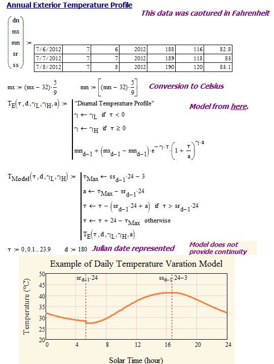
A reasonably simple model of daily temperature variation is given here. Figure 1 shows a screenshot of my Mathcad implementation.

Figure 1: Model of Daily Temperature Variation.

Figure 1: Model of Daily Temperature Variation.

Solar Load Modeling

To estimate the solar insolation, I need to model how the amount of solar energy varies throughout the day. Fortunately, these models are readily available and I use this one.

insolation. The results of my CFD modeling shows that our enclosure's internal ambient temperature rises by 19 °C over the air ambient in Phoenix at maximum solar insolation. Figure 2 shows the screenshot of my Mathcad version of this model.

Figure 2: Model of Enclosure Temperature Rise due to Solar Load  in Phoenix.

Figure 2: Model of Enclosure Temperature Rise due to Solar Load in Phoenix.

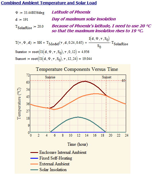
Combined Ambient Temperature and Solar Load Model

Figure 3 shows my combined ambient temperature and solar load model.

Figure 3: Combined Ambient Temperature and Solar Load Temperature Rise Model.

Figure 3: Combined Ambient Temperature and Solar Load Temperature Rise Model.

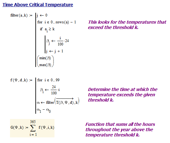
Summing Hours Enclosure Internal Ambient is Over 50 °C

Figure 4 shows my formulas for summing the hours over 50 °C during my model year.

Figure 4: Equations for Summing the Hours Greater Than a Threshold.

Figure 4: Equations for Summing the Hours Greater Than a Threshold.

Results

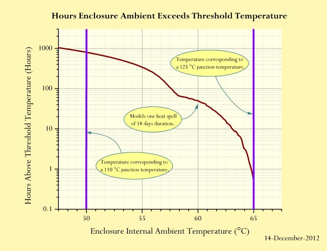
Figure 5 is the graphic that I generated to illustrate the number of hours that my enclosure's internal ambient exceeds 50 °C and other temperatures.

Figure 5: Projected Enclosure Internal Ambient Temperature Times.

Figure 5: Projected Enclosure Internal Ambient Temperature Times.

Conclusion

I am seeing that we will spend nearly 1000 hours per year above the 50 °C threshold temperature. This is more time than I would have expected. I will need to look at alternatives.

Posted in General Science | 6 Comments

Torpedo Data Computer Video

I am a fan of both naval history and the history of computing machines. I just saw a great video on the Torpedo Data Computer (TDC) that have I include here. The TDC was one of the last examples of an electromechanical analog computers. It played a major role in the Allied submarine war in the Pacific during World War 2.

If you wish more detailed information on the operation of the TDC, I have a number of posts on the topic. See these:

Some of you of a certain age may have seen analog computers in old science fiction movies. These films used analog computers as a kind of prop. The first analog computer I ever saw was a differential analyzer in When Worlds Collide. I am including a video here from Earth versus the Flying Saucers.

Not quite like the computer on Star Trek, but it did have nice penmanship.

Posted in Electronics, History of Science and Technology | 1 Comment

Network Cable Math

Introduction

Today I'm going to be discussing ethernet cables and if you've been reading this blog for a while, you know I'm no stranger to ethernet problems. I work with it quite a lot at work so I'm familiar with products like the ws-c2960s-48lps-l cisco catalyst and all the cables that ethernet entails. I am looking at category 5e (cat5e) cabling today. During some routine testing, I was seeing bit errors occurring on 100 meter long Ethernet cables that were operating at 60°C. This prompted me to investigate the effect of temperature on Ethernet bit error rate. Some businesses use a host server such as Hostiserver to minimise any faults and improve their web experiences. I found it surprising how complicated doing design work with these cables can be. In this post, I am going to review some basic cable characteristics and the kind of things that engineers need to look at when designing networks using these cables. There is nothing earth-shattering in this discussion -- things are just more complicated than you might expect. Let's dig in ...

Background

What Limits Cable Reach?

Most people think that the reach of Ethernet is 100 meters -- at true statement for a system operating at 20°C. We usually do not discuss what limits the reach of the cable. For the discussion at hand today, I will assume that signal attenuation limits the reach of the cable. There are other factors that can limit the reach of a system, but for today we will only look at signal attenuation.

The 100 meter reach number is based on some assumptions:

  • 90 meters of cat5e cable

    Cat5e cable is composed of 4 pairs of 24 American Wire Gauge (AWG) solid wires (8 wires total). The pairs are twisted to reduce the effects of electromagnetic interface. Unfortunately, the signal attenuates as it travels down the cable. The amount of attenuation is referred to as insertion loss.

  • 10 meters of cat5e patch cables

    Cat5e patch cables are composed of 4 pairs of 24 AWG stranded wires (8 wires total). The stranded wire is more flexible and is easier to bend than solid core wire, but it has higher insertion loss.

  • 4 connectors

    Connectors introduce additional losses that must be accounted for.

Communication systems are composed of transmitters, channels, and receivers. A minimum requirement for a reliable communication systems is for the transmitters to send a signal that is large enough for the receiver to clearly interpret after being attenuated by the channel.

Cat5e Attenuation Limits

The cat5e cable and connector attenuation limits are set by the industry standard TIA-EIA-568-B.2. I repeat these limits in Equation 1.

Eq. 1 \displaystyle I{{L}_{100mCable}}(f)\le 2.320\cdot \sqrt{f}+1.967\cdot f+0.050\cdot \frac{1}{\sqrt{f}}
\displaystyle I{{L}_{Connector}}\left( f \right)=0.040\cdot \sqrt{f}
\displaystyle I{{L}_{100mPatchCable}}\left( f \right)\le 1.2\cdot I{{L}_{100mCable}}(f)

where

  • IL100mCable is the insertion loss introduced by the 100 meters of cat5e cable (solid wire) at 20 °C.
  • IL100mPatchCable is the insertion loss introduced by the 100 meters of cat5e patch cable (stranded wire) at 20 °C.
  • ILConnector is the insertion loss introduced by a single connector at 20 °C.
  • f is the signal frequency expressed in MHz.

The industry has taken the approach that, as long as a cable has less attenuation than the specification's limit, enough signal from the transmitter will get through the channel to the receiver for reliable reception. Reliable reception is defined as a Bit Error Rate (BER) less than 1E-10.

Analysis

Insertion Loss @ 20 °C

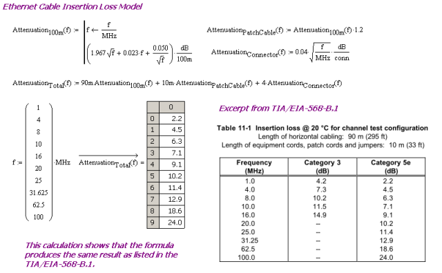
Figure 1 shows a screenshot of the Mathcad worksheet that I am using for my analysis. I have duplicated the insertion loss chart of TIA/EIA-568-B.1.

Figure 1: 100 meter Cat5e Insertion Loss Calculation.

Figure 1: 100 meter Cat5e Insertion Loss Calculation.

Insertion Loss Increase at Higher Temperature

TIA-EIA-568-B-1 specifies how the insertion loss calculations are to be performed at elevated temperatures. Cable loss is to modeled as a 0.4% per °C increase in temperature. For the exact quote, see Appendix B. Since all the losses are multiplied by 0.4%/°C and we must keep the insertion loss under the 20 °C value at all frequencies, the maximum reach of Ethernet reduces by 0.4%/°C. So if we run our Ethernet over 60 °C cable, the maximum range is reduced by 16 meters. The calculation is shown in Equation 2.

Eq. 2 100\text{ meters }\cdot \left( 60\text{ }^\circ\text{C}-20\text{ }^\circ\text{C} \right)\cdot \frac{0.4\%}{^\circ\text{C}}= 16 \text{ meters }

Conclusion

It appears that the increased temperature I am encountering with this cabling is reducing the maximum length supported by Ethernet. I will need to adjust my test configurations.

Appendix A: Quote on Stranded Cable Insertion Loss Tax

The following quote from TIA-EIA-568-B-1 addresses the modeling approach to be used for cat5e patch cables.

Cat 5e stranded cable table shall meet the values computed by multiplying the horizontal cable insertion loss requirement in clause 4.3.4.7 by a factor of 1.2 (the de-rating factor), for all frequencies from 1 MHz to 100 MHz. The de-rating factor is to allow a 20% increase in insertion loss for stranded construction and design differences.

Appendix B: Quote on Cat5e Insertion Loss Increase with Temperature

The following quote from TIA-EIA-568-B-1 addresses the modeling approach to be used for cat5e patch cables.

Insertion loss is expressed in dB relative to the received signal level. Insertion loss shall be measured for all cable pairs in accordance with ASTM D4566 and 4.3.4.14 at 20 ± 3°C or corrected to a temperature of 20 °C using a 0.4%/°C correction factor for category 5e cables for the measured insertion loss.

Posted in Electronics | 7 Comments

Crest Factors for QAM Signals

Quote of the Day

If you want to succeed you should strike out on new paths, rather than travel the worn paths of accepted success.

— John D. Rockefeller


Introduction

I need to do a quick calculation of the Crest Factor (CF) for various types of Quadrature Amplitude Modulation (QAM) signals. CF is important to a hardware designer because higher CF values generally means more expensive components in order to meet the demand for high peak currents (or voltages) relative the the power delivered. As always, I first went to the Wikipedia to check out what they had on the subject. Unfortunately, the Wikipedia's article on CF only listed the QAM-64 CF (Note - I have since updated that Wikipedia page). Looks like I will need to compute the CFs for the other QAM options that I am interested in. I am sure they are in a reference somewhere, but I am short of time.

While performing this calculation, I decided to see if Mathcad's symbolic solver could give me a general equation for the CF of a QAM signal with a perfect square number of signal symbols (i.e. QAM-N2). It gave me a reasonable result that also produces a result for QAM-∞ that is the same as is listed in the Wikipedia.

Background

As far as information on QAM, Wikipedia's article on QAM is better than anything that I could write here.

The calculation on CF for a QAM signal is straightforward. Engineers normally discuss QAM signals in terms of a constellation diagram. Figure 1 shows a constellation diagram for QAM-16.

Figure 1: QAM-16 Constellation Diagram from Wikipedia.

Figure 1: QAM-16 Constellation Diagram from Wikipedia.

Crest Factor is defined as shown in Equation 1.

Eq. 1 \displaystyle CF=\frac{|x{{|}_{\text{peak}}}}{{{x}_{\text{rms}}}}

where

  • CF is the crest factor of the signal x (unitless)
  • xRMS is the RMS value of the signal x.
  • \displaystyle |x{{|}_{\text{peak}}} is the peak of the signal x.

CF can be computed for either currents or voltages. My focus here will be on voltages.

Analysis

Computational Approach

I need to compute the CF for QAM-4, QAM-16, QAM-64, and QAM-256. If I assume that all signals in the constellation are equally probable, the calculation is straightforward. Figure 2 shows my calculation in Mathcad. The numerator of my CF calculation is the maximum amplitude of the set of possible QAM signals. The denominator contains the RMS calculation for all the possible QAM signals assuming that they are equally likely. I also can ignore the absolute amplitudes of the various QAM signals because I am working with ratios.

Figure 2: Screenshot of my Mathcad Calculation of QAM Crest Factors.

Figure 2: Screenshot of my Mathcad Calculation of QAM Crest Factors.

These values make sense (i.e. agree with what I know to be true for QAM-4 and the Wikipedia entry for QAM-64). Figure 3 shows a plot of CF versus QAM constellation size.

Figure 3: Crest Factor Versus Constellation Size.

Figure 3: Crest Factor Versus Constellation Size.

Symbolic Analysis

I took the formula shown in Figure 2 and assumed a symbol number of N2, where N is an even number. Figure 4 shows the result of this symbolic analysis.

Figure 4: General Solution for Constellations with N<sup>2</sup> Symbols.

Figure 4: General Solution for Constellations with N2 Symbols.

Note that for constellations with a large number of symbols, the CF approaches \displaystyle \sqrt{3}.

Conclusion

Quick, simple calculation that solved my problem. I have added three appendices:

  • Appendix A that includes examples of square and non-square constellation configurations.
  • Appendix B shows one way of computing the crest factors for both square and non-square constellations.
  • Appendix C shows an excerpt from a reference that derives the same general equation as presented here.

Appendix A: Constellation Examples

Figure 5 shows some constellation examples. Note how the non-square constellations have their corners cutoff. Other configurations are possible and each will have different crest factors.

Figure 5:QAM Constellation Examples.

Figure 5:QAM Constellation Examples.

Appendix B: Crest Factor and PAR Calculation for Non-Square Constellations

Figure 6 shows an example of how I computed the crest factor and PAR for both square and non-square constellations. Calculations are more tedious for non-square constellations because of the need to manually cutoff the corner points.

Figure 6: Alternative Calculation that Handles Square and Non-Square Cases.

Figure 6: Alternative Calculation that Handles Square and Non-Square Cases.

These numbers agree with the table included in this here.

Appendix C: Reference that Discusses Crest Factor for Square Constellation Sizes

Figure 7 shows a reference that I found that presents a general formula for Peak-to-Average Power Ratio (PAPR), which equals CF2. The answers are the same as I present here.

Figure 7: Statement of General Solution for Square Constellations.

Figure 7: Statement of General Solution for Square Constellations.

Posted in Electronics | 22 Comments

Trapezoids Better Than Sinusoids?

Quote of the Day

The worst enemy of life, freedom and the common decencies is total anarchy; their second worst enemy is total efficiency.

— Aldous Huxley


Introduction

Figure 1: Trapezoidal Specification Example. (Source)

Figure 1: Trapezoidal Specification Example. (Source)

Sinusoids hold a revered place in electrical engineering -- they should. However, I do encounter quite a few trapezoids in telecom power systems. During a meeting the other day, I was asked "Why do we use trapezoidal waveforms for Alternating Current (AC) signals like ringer voltages and remote power systems." It was a good question. I have written about the trapezoidal waveform before, but I have never explained why the trapezoid is used so frequently.

As with most engineering tradeoffs, our constant quest for lower cost at a specified level of performance will drive the answer. Let's dig in ...

Background

Assumptions

To simplify this discussion, I will assume that we are evaluating the relative merits of two types of AC power system output waveforms, sinusoidal and trapezoidal. Figure 2 shows my simple model for a trapezoidal power system. The sinusoidal model is identical except for replacing the trapezoidal waveform with a sinusoidal waveform.

Figure 1: Trapezoidal Power System Model.

Figure 2: Trapezoidal Power System Model.

The choice of power source waveform will have an impact on the load power converter's cost. Because there are far more loads in telecom systems than sources, the total system cost is usually driven by the cost of the load hardware. Thus, it is important to choose a power source waveform that will reduce the cost of the load's power converter.

I am going to ignore any cost differences in generating trapezoids versus sinusoids. The Total Cost of Ownership (TCO) for the system is dominated by the large number of loads, so a bit more cost in the generator is more than made up by the lower cost of the loads.

Key Idea

The TCO for power conversion systems is driven by their installed cost, operating efficiency, and failure rate. Systems that have high peak currents relative to their RMS input currents have a higher TCO than systems with lower peak to RMS input current ratio. The ratio of peak to RMS current is called the Crest Factor (CF). While I will focus on the CF for currents here, similar statements can be made for voltages as well. I focus on the current CF here because it is larger than the voltage CF. Power systems with diodes in them tend to see high current peaks because of the exponential dependence of diode current on diode voltage.

I can give you a number of examples as to why high CF drives system cost:

  • Capacitor Reliability

    The reliability of aluminum electrolytic capacitors are reduced when they must support large ripple voltages. High CF tends to create high ripple voltages across these capacitors.

  • Conversion Efficiency

    Systems with high CF have relatively high peak currents, which also results in RMS currents that are significantly higher than the average current draw. High RMS currents increase resistive losses in teh system, making the overall conversion efficiency lower. The lower conversion efficiency increases the total cost of ownership of the system by driving up annual operating costs.

  • Power Dissipation

    Power dissipation increases the load's operating temperature, which results in lower reliability.

  • Component Cost

    The cost of many components, like diodes, is driven by the peak current they must handle.

Ideally, we want to choose the voltage waveform that will minimize the CF level. The trapezoidal waveform is easy to generate and reduces the CF level in the system.

Some Definitions

We need to provide some precise definitions of the following terms.

Crest Factor (CF)
The crest factor is a waveform metric that is calculated from the peak amplitude of the waveform divided by the RMS value of the waveform. Mathematically, we compute crest factor using CF=\frac{|f{{|}_{\text{peak}}}}{{{f}_{\text{rms}}}}, where f represents the waveform. We can compute CF for either current or voltage. In this note, I focus on currents.
Peak Current (I_{Peak})
Peak current is the maximum current at which the product must meet its requirements.
Peak Voltage (V_{Peak})
Peak voltage is the maximum voltage at which the product must meet its requirements.
Root-Mean-Square (RMS)
The RMS value of continuous-time parameter is the square root of the arithmetic mean of the square of the function that defines the continuous parameter. Mathematically, we compute the RMS value using {{f}_{\text{rms}}}=\underset{T\to \infty }{\mathop{\lim }}\,\sqrt{\frac{1}{T}\int_{0}^{T}{{{[f(t)]}^{2}}}dt}, where f(t) is the continuous-time parameter (usually voltage or current). The RMS value of a waveform is always greater than or equal to its average. The proof is here.

Analysis

Rectified Input Characteristics

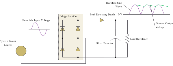
Most telecom loads use some form of bridge rectifier at their power input. Figure 3 shows a typical example.

Figure 2: Rectified Output Voltage.

Figure 3: Rectified Output Voltage.

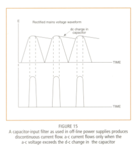
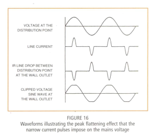
The rectification process causes the input current draw to appear in the form of spikes that occur when the input waveform is at its peak. The input spikes occur because the input only draws current when the input voltage is higher than the voltage on the output capacitor. I found a couple of nice illustrations of this action on this web site and I repeat them here in Figure 4.

Figure 4: Excellent Illustration of the Input Current Draw Characteristics of a Rectified Input
Illustration of the Input Current Draw Spikes Input Current Draw and it Effect on the Input Waveform.

Example Circuit

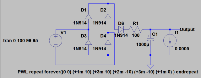
Rather than use mathematics to beat this problem to death, I thought I would just perform a simulation. I downloaded the free simulator LTspice and put in a simple example circuit. This circuit is completely made up just for use in this example, so do not send me email telling me that there are better components I could use.

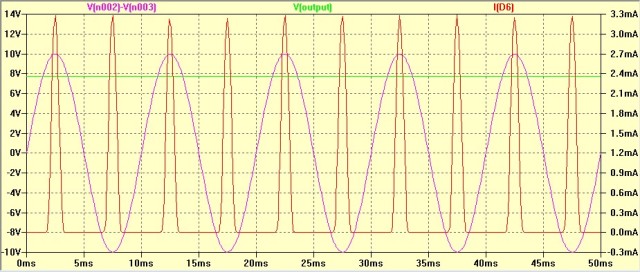
Figure 5 shows the LTspice simulation for the case of a sinusoidal input (10 V amplitude at 100 Hz). The circuit has a 0.5 mA current source for its output load.

Figure 4: Simulation Schematic for a Sinusoidal Input Voltage.

Figure 5: Simulation Schematic for a Sinusoidal Input Voltage.

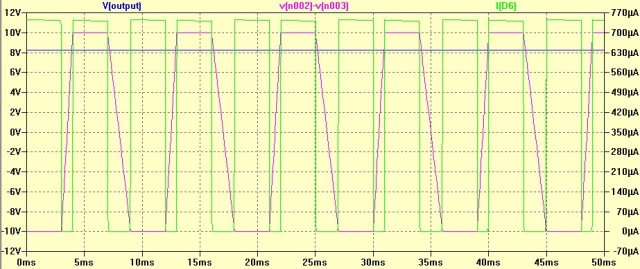
Figure 6 shows the LTspice simulation for the case of a trapezoidal input (10 V amplitude at 100 Hz). The circuit has a 0.5 mA current source for its output load.

Figure 5: Schematic Configured for a Trapezoidal Input Voltage.

Figure 6: Schematic Configured for a Trapezoidal Input Voltage.

Simulation Results

Figure 7 shows the simulation results for the sinusoidal test case. Notice that the input current peaks at ~3.3 mA even though the actual output current is only 0.5 mA.

Figure 6: Simulation of the Rectifier Circuit with a Sinusoidal Input.

Figure 7: Simulation of the Rectifier Circuit with a Sinusoidal Input.

Figure 8 shows the simulation results for the trapezoidal test case. Notice that the input current peaks at ~0.820 mA, which is much less than the 3.3 mA peak for the sinusoidal test case.

Figure 7: Simulation of the Rectifier Circuit with a Trapezoidal Input.

Figure 8: Simulation of the Rectifier Circuit with a Trapezoidal Input.

Conclusion

Table 1 summarizes the results from my simulation effort. The actual calculations are a tad boring, but I have captured them in Appendices A and B.

Table 1: Summary of Average, RMS, and Peak Current Values By Input Waveform
Waveform Type Average Input Current (mA) RMS Input Current (mA) Peak Input Current (mA) Crest Factor
Sinusoidal 0.500 1.105 3.244 2.936
Trapezoidal 0.500 0.575 0.743 1.293

We can see from Table 1 that the crest factor is much lower for a trapezoidal input signal than for a sinusoidal input signal. This means the the cost of component can be minimized and the overall reliability improved if we use a trapezoidal waveform for our AC voltage waveform.

Appendix A: Average, RMS, and Peak Current Values for the Sinusoidal Input Waveform.

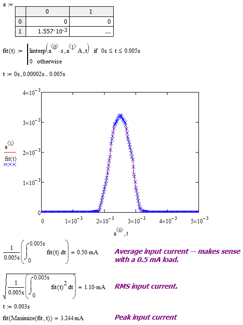
Figure 9 shows an example of basic sine wave current calculations.

Figure 8: Screenshot of Mathcad Worksheet Calculations for Average, RMS, and Peak Input Current Using a Sinusoidal Input Waveform.

Figure 9: Screenshot of Mathcad Worksheet Calculations for Average, RMS, and Peak Input Current Using a Sinusoidal Input Waveform.

Appendix B: RMS and Peak Current Values for the Trapezoidal Input Waveform.

Figure 10 is similar to Figure 9, but for a trapezoidal waveform.

Figure 9: Screenshot of Mathcad Worksheet for RMS and Peak Current Using a Trapezodal Input Waveform.

Figure 10: Screenshot of Mathcad Worksheet for RMS and Peak Current Using a Trapezoidal Input Waveform.

Save

Save

Save

Save

Posted in Electronics | 7 Comments

Design Review of Four Transistor Current Source

One of the engineer's in my group asked if I had any information on how a four transistor current source works. I decided that to pull together a quick Mathcad worksheet. The Wikipedia refers to this current source configuration as a four-transistor improved current mirror. Figure 1 shows an image of this circuit from the Wikipedia.

Figure 1: Four-Transistor Improved Current Mirror (Source: Wikipedia).

Figure 1: Four-Transistor Improved Current Mirror (Source: Wikipedia).

I have attached a PDF version of the Mathcad worksheet and included a link to Mathcad 15 source in a zip file. There is a macro in it that just generates the table of contents.

Posted in Electronics | 3 Comments

Quadrature Modulators Solve Old Problems with Self-Calibration

Introduction

I was reading EETimes this month when I saw an interesting article on analog quadrature modulators (AQMs). I have not looked at these devices in a while and I noticed that some of my early issues with AQMs may not be a problem anymore. My issues had to do with the sensitivity of AQMs to small errors -- DC offsets and small phase errors. Today's versions of these circuits incorporate self-calibration capabilities that eliminate my previous concerns. The article is a good one and worth reading closely.

As I usually do, I wrote up a Mathcad worksheet as I read the article so that I could duplicate their analysis and make sure that I understand the material. This post is based on this worksheet. My design data package (i.e. all data associated with an electronics design) typically contains a number of these worksheets that describe component operation and design details.

This analysis effort is not just an academic one for me -- I actually have a home project where one these devices will be very useful.

Background

When I think of quadrature modulators, I usually think of the Weaver single-sideband (SSB) modulator shown in Figure 1, which is intended to produce the lower SSB signal. All of the discussion to follow will assume that the lower sideband is desired and the upper sideband is not. The argument can easily be flipped for an upper SSB system.

Figure 1: SSB (Lower) Generation Using the Weaver Modulator.

Figure 1: SSB (Lower) Generation Using the Weaver Modulator.

I list here some of the key points about the Weaver modulator:

  • The left-hand side of Figure 2 simply converts the input signal into its in-phase and quadrature components.

    I will not be spending any further time on this section. The Wikipedia does have a discussion of the concept.

  • The right-hand side actually generates the single sideband version of the input signal.

    This portion of the circuit is the focus of my discussion here.

  • The right-hand side will generate the lower sideband or upper sideband depending on whether you have a sum or difference function at the output, respectively.

    You can easily see how the upper sideband can be generated by changing the plus sign on the right-hand side of Equation 1 to a minus.

I always liked the visual symmetry of the Weaver modulator. Its operation is easy to understand because it represents the physical realization of a trigonometric formula, which I show in Equation 1. Its operation is well described using the product-to-sum trigonometric formulas.

Eq. 1 \displaystyle \cos \left( {{\omega }_{C}}\cdot t \right)\cdot \cos \left( {{\omega }_{B}}\cdot t \right)+\sin \left( {{\omega }_{C}}\cdot t \right)\cdot \sin \left( {{\omega }_{B}}\cdot t \right)=
\displaystyle \frac{1}{2}\cdot \cos \left( \left( {{\omega }_{C}}-{{\omega }_{B}} \right)\cdot t \right)+\cos \left( \left( {{\omega }_{C}}+{{\omega }_{B}} \right)\cdot t \right)
\displaystyle +\frac{1}{2}\cdot \cos \left( \left( {{\omega }_{C}}-{{\omega }_{B}} \right)\cdot t \right)-\cos \left( \left( {{\omega }_{C}}+{{\omega }_{B}} \right)\cdot t \right)
\displaystyle =\cos \left( \left( {{\omega }_{C}}-{{\omega }_{B}} \right)\cdot t \right)

where

  • ωC is angular frequency of the carrier.
  • ωB is the angular frequency of the baseband signal.

The Weaver modulator is often used today in digital realizations of SSB modulators. However, 30+ years ago (i.e. back in my day), EE professors warned their students to beware of analog implementations of this circuit because it is sensitive to the various DC and phase errors that occur in analog systems. If you look at Equation 1, their warning makes sense. Because analog electronics always has small DC offsets, the carrier will not be perfectly cancelled out -- an effect usually referred to as carrier leakage. Similarly, small phase errors will mean that the upper sideband will not be completely cancelled out -- sort of a sideband leakage. These errors used to take an enormous amount of effort to remove. Things are different today. We can put circuitry on the modulator chips that can introduce compensating DC and phase errors that will nearly eliminate the upper sideband leakage.

To model these errors, I will focus on the modulator portion of Figure 1, which I expand for easier viewing in Figure 2.

Figure 2: Quadrature Modulator Model.

Figure 2: Quadrature Modulator Model.

Analysis

DC Offset

I go through modeling the effect of DC offsets in Figure 3, which shows how we can:

  1. Introduce DC offsets into the in-phase (DCi) and quadrature inputs (DCq).
  2. Simplify the resulting expression to show that the modulator produces a desired term at ωC - ωB and an undesired term at ωC.
  3. Show the magnitude of the undesired term is \sqrt{DC_{i}^{2}+DC_{q}^{2}}.

Figure 3: Modeling the Effect of a DC Offset on Quadrature Modulation.

Figure 3: Modeling the Effect of a DC Offset on Quadrature Modulation.


Figure 4 illustrates the process of reducing the effect of the DC offsets by introducing compensating offsets using step-wise refinement:

  1. [red line] Introduce DC shifts into the in-phase path and find the offset that minimizes the carrier leakage.
  2. [blue line] Applying the in-phase DC shift determined above, introduce DC shifts into the quadrature-phase path and find the offset that minimizes the carrier leakage.
  3. [pink line] Applying both the in-phase and quadrature DC shifts determined above, again find the new in-phase offset that minimizes the carrier leakage. This update should be small.
  4. [green line] Applying both the updated in-phase and quadrature DC shifts determined above, again find the new quadrature-phase offset that minimizes the carrier leakage.

The example in the article and in my Figure 4 iterated four times. In theory, you will iterate until you get the error down to the level your application requires.

Figure 4: Step by Step Removal of the Carrier Leakage.

Figure 4: Step by Step Removal of the Carrier Leakage.

In the Figure 4 example, you will see that I add a small random component to the measured carrier leakage. The original article mentioned that noise caused the minimization algorithm to take multiple passes. The addition of a small amount of noise in the leakage model confirms that statement.

Phase Errors

The effect of phase errors in the system are modeled by the Sideband Suppression ratio (SBS), which I show in Equation 2.

Eq. 2 \displaystyle SBS({{G}_{LO}},\phi )=10\cdot \log \left( \frac{1+{{\left( 1+{{G}_{LO}} \right)}^{2}}+2\cdot \left( 1+{{G}_{LO}} \right)\cdot \cos \left( \phi  \right)}{1+{{\left( 1+{{G}_{LO}} \right)}^{2}}-2\cdot \left( 1+{{G}_{LO}} \right)\cdot \cos \left( \phi  \right)} \right)

where

  • GLO the gain error (i.e. difference from 1) in the local oscillator relative to the input path.
  • φ the phase shift of the local oscillator relative to the phase shifts present in the input path.

Figure 5 shows how we can go about deriving Equation 3.

Figure 5: Derivation of Sideband Suppression Ratio Equation.

Figure 5: Derivation of Sideband Suppression Ratio Equation.


We can now plot Equation 2 versus phase and gain errors using a contour plot (Figure 6).
Figure 6: Sideband Suppression Contour Plot Versus Phase Error and Amplitude Error.

Figure 6: Sideband Suppression Contour Plot Versus Phase Error and Amplitude Error.

Conclusion

This post is a discussion of a magazine article that was about a circuit that I intend to use shortly in a home project. It was interesting to see how a circuit architecture that used to have serious problems has now evolved in a very simple way to minimize these problems.

Posted in Electronics | Comments Off on Quadrature Modulators Solve Old Problems with Self-Calibration

What Does It Mean to be an Expert?

As an engineering director, I must annually review my employees for performance relative to the standards of their assigned job categories. If an employee is performing above or below their assigned standards, their job category may need to be changed. This task is important to an employee because it affects their pay. All corporations that I know of pay their employees based upon the job category that the employees are assigned to. To make it easier for me to control who is earning what, I need a reliable Payroll Software to help make this an organised process. Gone are the days where you would hand a pay packet to your employees each month, everything now is basically digital and will be transferred via trusted payroll software. For example, using ach payment processing for small business can set a business apart from those who do not want to advance with new technologies.

My tale today involves defining the word "expert." The rubric for one of our job categories requires it members to be a "recognized expert in their field." I have been mulling over what it means to be an expert. My own imprecise definition is someone who is a master of their field and who is recognized by others as such. So if I wanted to hire an expert cloud architect engineer, how would I select the expert from a sea of candidates? Would simply having a google cloud architect certification make an expert of someone? Or does it require something more? Let's see if I can put a finer edge on my definition.

Since I know others have had these questions before me, I started my research with a Google search. After a bit of time, I saw a very interesting reference on this blog -- by the way, a great blog on teaching statistics and design of experiments. It makes sense that educators would be thinking about the definition of an expert.

The reference is named "How People Learn: Brain, Mind, Experience, and School." They define an expert as having the following characteristics. I agree with each characteristic listed.

  • Experts notice features and meaningful patterns of information that are not noticed by novices.
  • Experts have acquired a great deal of content knowledge that is organized in ways that reflect a deep understanding of their subject matter.
  • Experts' knowledge cannot be reduced to sets of isolated facts or propositions but, instead, reflects contexts of applicability: that is, the knowledge is "conditionalized" on a set of circumstances.
  • Experts are able to flexibly retrieve important aspects of their knowledge with little attentional effort.
  • Though experts know their disciplines thoroughly, this does not guarantee that they are able to teach others.
  • Experts have varying levels of flexibility in their approach to new situations.

Since there are people who wish to advance into the job category that requires them to be an expert, I need to give them some guidance on how to become an expert. After some additional web searching, I saw a quotation from Willy Sansen, whose original work was titled ‘"Solid-state circuits and a career for life." His work was quoted on this blog. He was answering the question -- What advice can be given to students who want to build up a career in solid-state circuits? His advice is struck me as being true for every profession at some level.

  1. To be successful in a career, maintain a very specific field of expertise.

    Too often a designer runs through many designs, to find himself in a corner where he knows a little bit about everything. He must, instead, strive to be number one in the world in a specific field of expertise as if it were a hobby, to keep himself wanted on the market.

  2. Be known as an expert.

    Present papers at conferences or workshops, or publish papers or abstracts. Nobody is an expert unless he is accepted as an expert.

  3. Become an expert on an international level.

    The time is gone when an expert could be an expert in his little corner; globalization has flattened this world. The competition may be close by, but could also be on the other side of the earth. The designer must thus be accepted by experts everywhere.

  4. Give presentations to colleagues, to your boss, to students.

    Transferring knowledge from one person to another is an art. Only by doing so regularly, can a designer be efficient in making clear why he is an expert.

There is some gold to be mined here. As far as item (1) goes, I am afraid that most technical fields today are so rich in content that an engineer must focus their energy in order to develop an significant level of expertise. My field, electronics, is so broad today that I have had to focus on analog electronics and optics.

Notice how items (2)-(4) are all about technical communications. From my standpoint, you do not have to be internationally recognized to be an expert -- Susan Boyle was an expert singer before she was internationally recognized. An expert cannot give the title to themselves, they must earn the title with the respect of their peers. Many have to face multiple trials and tribulations, uploading their songs on apps like YouTube and SoundCloud, while getting little to no recognition. Few even turn to YouTube and Soundcloud promotion websites to get a few followers! However, many engineers do not understand that some level of career marketing is necessary in order to advance. I have known many fine engineers who felt that their expertise should be recognized without any communications effort from them. They never got anywhere.

I think I understand how to become a recognized expert:

  1. Develop deep knowledge in an area that is broad enough to be of interest to your peers, but narrow enough that you can actually master it.
  2. Learn how to communicate your knowledge to others.
  3. Take advantage of opportunities to become an advocate for your chosen area of study -- participate in trade associations, shows, conferences, and workshops.

I think this is the approach I will recommend to the folks in my group.

Posted in Management | 1 Comment

Skydiving Math

Introduction

I must admit that I was amazed at what Felix Baumgartner accomplished. As I watched the video, I found myself focusing on the video's display of Felix's speed versus time. It was really interesting to see how he quickly he accelerated to faster than Mach 1 speed and then he began to decelerate as he hit denser atmosphere. The video below is the one I was watching.

https://www.youtube.com/watch?v=7f-K-XnHi9I

As I thought about, I could compare Felix's speed versus time data with the predictions from a differential equation. This gives me another opportunity to try out Mathcad Prime 2.0. Let's dig in ...

Background

My approach to this problem is simple:

  • Capture the empirical data from the jump video and put it into Mathcad Prime.

    This was the only routine and boring part of the exercise.

  • Capture data from NASA on the atmosphere's density and the variation in gravity with altitude.

    I used this same file for my post on Mars's atmosphere.

  • Create a differential equation model and use Mathcad Prime to solve it.

    I will use the high-speed drag model shown in the Wikipedia to keep things simple. I have used a more sophisticated drag model in a previous blog post, but I wanted to keep this one simple. Since Felix was spinning and changing position, his coefficient of drag was changing -- modeling it as a constant is sure to be wrong. I am just looking for an approximate model. However, it may provide some insight into what was going on.

  • Tune the differential equation model's coefficient of drag (defined below) to best match the empirical data

    I am constantly performing optimizations at work. I might as well start getting used to optimizations in Mathcad Prime.

  • Compare the empirical data to the tuned differential equation model and see how well the mathematics compares to reality.

    Here is where I get practice with the graphics in Mathcad Prime.

Analysis

Empirical Speed Capture

My approach to capturing the speed data was simple.

  • Watch this video.
  • Write down the numbers for times and speeds that I see on the video.

I am afraid sometimes you just have to sit there and write stuff down by hand. There are problems with gathering the data this way.

  • The data is quantized in one second intervals.
  • Sometimes the data changes two or three times during a single one second interval.
  • The speed data may also be quantized -- the speed numbers are not changing continuously.

What this means is that the data I took by hand suffers from quantization errors (both in amplitude and timing). To minimize these errors, I will both smooth and interpolate the my rough speed and time readings.

Figure 1 shows how the data looks in Mathcad Prime 2 after I did my post-processing.

Figure 1: Video Data Captured, Smoothed, Interpolated, and Plotted in Mathcad Prime 2.0.

Figure 1: Video Data Captured, Smoothed, Interpolated, and Plotted in Mathcad Prime 2.0.

Modeling Atmospheric Density and Gravity

This data comes straight from NASA and all I am doing is running the data through an interpolation routine. Figure 2 shows how this interpolation looks in Mathcad Prime.

Figure 2: NASA Data on the Atmosphere's Density and Gravity Variation with Altitude.

Figure 2: NASA Data on the Atmosphere's Density and Gravity Variation with Altitude.

Atmospheric Drag Modeling

The skydiver experiences two forces during his fall:

  • atmospheric drag
  • gravity

These two forces are combined into a single differential equation. Let's first review the effects of both drag and gravity.

The Wikipedia has a very good discussion of drag for those readers requiring more background. I will use Equation 1 from this article to model the force of drag on the skydiver.

Eq. 1 \displaystyle {{F}_{D}}=\tfrac{1}{2}\cdot \rho \cdot {{v}^{2}}\cdot {{C}_{d}}\cdot A

where

  • FD is the force of drag [N]
  • A is the cross-sectional area presented to the air stream [m2]
  • ρ(x) is the density of the atmosphere as a function of altitude [kg/m3] -- from here
  • CD is the coefficient of drag [unitless]
  • v is the velocity of the skydiver [m/s]

Gravity Modeling

Modeling the force of gravity is simpler than modeling drag, but we will increase the complexity just a tad by incorporating its variation with altitude. While this is a small effect, it does provide for a more complete model. Equation 2 shows the mathematical model I will be using.

Eq. 2 \displaystyle {{F}_{G}}=m\cdot g(h)

where

  • m is the mass of the skydiver and equipment [kg]
  • g(h) is the acceleration due to gravity as a function of height [m/s2]

I will use a guess for the mass of the skydiver (m=100 kg), and I will obtain the gravitational acceleration as a function of height from this document.

Overall Differential Equation

With both drag and gravity modeled, we can now write down the full differential equation (Equation 3).

Eq. 3 {{F}_{Total}}=-m\cdot g(h)+\tfrac{1}{2}\cdot \rho \cdot {{v}^{2}}\cdot {{C}_{d}}\cdot A

With this equation, we can now setup our differential equation solver, which I show in Figure 3.

Figure 3: Setup of the Differential Equation Solver.

Figure 3: Setup of the Differential Equation Solver.

Optimizing My Estimate for the Coefficient of Drag

I have no idea what the coefficient of drag is for a skydiver wearing a pressure suit. I will use an optimization routine to determine the coefficient of drag that best matches the empirical speed data. Figure 4 shows how this optimizer was setup.

Figure 4: Setup of the Coefficient of Drag Optimizer.

Figure 4: Setup of the Coefficient of Drag Optimizer.

Results

Figure 5 shows the comparison between my mathematical model and the empirical speed data.

Figure 5: Comparison Between Mathematical Model and Empirical Data.

Figure 5: Comparison Between Mathematical Model and Empirical Data.

Conclusion

The empirical data and the output of the mathematical model are very similar. At this point, I think I understand the modeling. It really is remarkable how good a simple model can be. The exercise also proved to be a good exercise in the use of Mathcad Prime 2.0.

Appendix A: Mathcad Source File

Here is the Mathcad Prime 2.0 file that was used to make this blog post.
Skydiving.mcdx
This is an XML file. Just download it to your desktop and open it up with Mathcad. For those without Mathcad, here is the PDF version.
Skydiver.pdf

Posted in General Mathematics, General Science | 1 Comment

Not Every Scientist Starts Out a Prodigy

Quote of the Day

A father is only as happy as his least happy child.

- Dr. Phil. This is something a dad understands.


NobelPrizeReportCardI have to share this news story about John Gurdon, who is one of the 2012 Nobel Prize Winners in Medicine. He was no prodigy -- in fact, he had issues in school. The news article contained an image of one of his school report cards. His early performance did not bode well for his future in science. In fact, one Biology report card comment was so harsh that I thought it was worth putting into my quote database (I have a database for everything).

It has been a disastrous half. His work has been far from satisfactory. His prepared stuff has been badly learnt, and several of his test pieces have been torn over; one of such pieces of prepared work scored 2 marks out of a possible 50. His other work has been equally bad, and several times he has been in trouble, because he will not listen, but will insist on doing his work his own way. I believe he has ideas about becoming a Scientist; on his present showing this is quite ridiculous, if he can't learn simple Biological facts he would have no chance of doing the work of a Specialist, and it would be sheer waste of time, both on his part, and of those who have to teach him.

I have known a number of people whose performance in school bore no resemblance to their performance on the job. I have always wondered about what causes these differences in performance. After three decades in engineering, I am no closer to the answer.

Posted in General Science, Management | 2 Comments