
Quote of the Day
You have to perform at a consistently higher level than others. That's the mark of a true professional.
— Joe Paterno
Introduction

Figure 1: Typical Avalanche Photodiode. (Source)
During a meeting recently, a vendor was discussing the need for performing production calibration testing that required fitting a parabola to the data from an optical sensor called an Avalanche PhotoDiode (APD) (Figure 1). I recalled this comment while reviewing a test report this morning where I saw a parabola appear in an APD test report from an optical physicist in my group. I realized that our physicist and this vendor were working in related areas. It was an excellent test report that covered both the theoretical and experimental aspects of the subject. It also seemed like a good topic for this blog.
I thought this was a good example of a common situation in electronics:
- You need to determine a physical parameter (e.g. average optical power) that is a function of some electrical parameter (e.g. voltage across a resistor).
- The parameter is a nonlinear function of the electrical parameter -- in this case, the nonlinear function is a parabola.
- Each component will have a slightly different nonlinear function that must be determined during the production testing for each part.
- You want to minimize the amount of production data you must gather because the cost of gathering data increases with the amount of data.
This post will provide a brief description of how an APD is used in a optical receiver circuit and how we can measure the average optical power received by the APD.
Background
Optical Networks
My group builds Optical Network Units for GPON systems. The ONUs are mounted on the sides of homes and they contain both optical transmitters (i.e. lasers) and receivers (i.e. APDs). The APDs detect the light pulses on the fiber that convey information to the home. APDs are capable of detecting very small changes in light level -- in fact, they can even count individual photons when the used in the correct circuit. In this particular case, we want to measure average optical power and not instantaneous power.
The whole concept of using avalanche phenomena to create very sensitive detectors is an old one. APDs are very similar in concept to the Photomultiplier Tube (PMT). Geiger counters also use similar technology.
APD Background
For our work here, I am going to treat the APD as a mathematical object -- no circuit details. These details are not need to understand how we can measure average optical power using a photodiode. For our purposes here, there are three things we need to know about APDs:
- They convert optical power into current.
- The conversion factor between optical power and current is a function of the voltage applied to the APD.
- The conversion factor is a highly nonlinear function of the voltage applied to the APD.
Equation 1 is the key equation showing the relationship between optical power and APD current.
| Eq. 1 |  |
where
- IAPD is the current through the APD.
- VAPD is the voltage across the APD. This voltage is set during production to provide the desired level of amplification.
- M(VAPD) is an adjustable gain (i.e. multiplication) factor. This is useful because we need to ensure that current from the APD is kept within the range of values that our electronics can measure.
is the responsivity of the photodiode. It is a conversion factor from optical power (Watts) into current (Amperes).
The multiplication factor, M(VAPD), is described by Miller's formula, which I state in Equation 2.
| Eq. 2 | 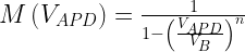 |
where
- VB is the breakdown voltage of the APD. This is a critical parameter for all APDs.
- n is a parameter that varies with the design of the specific device. We will assume n=1 for our work here.
During manufacturing, we adjust VAPD to achieve the desired gain. The setting of the gain is always a "Goldilock's Problem" -- the gain must be high-enough so that you can detect the minimum signal level you expect to encounter, but not so high that you saturate your detector with the maximum signal level you expect to encounter.
Current Mirror
The Wikipedia has a good working definition of a current mirror.
A current mirror is a circuit designed to copy a current through one active device by controlling the current in another active device of a circuit, keeping the output current constant regardless of loading.
In the case here, our current mirror actually makes a duplicate of 1/5 of the APD current. This scaling is useful because the APD current range is so wide that it is difficult to measure accurately without reducing its range.
Analysis
Schematic
Figure 2 is a simplified schematic of the receiver circuit. The circuit here is based on one in a Maxim application note. There are different ways of implementing receivers, but this is a reasonable one.

Figure 2: Simplified Schematic of the Optical
Figure 2 deserves a few comments:
- VOut is connected to the input of an A/D converter.
The A/D converters have a limited range of voltages that they can convert. A typical range would be 0 V - 2.00 V. The current in the APD will increase as the APD receives more optical power.
- CBypass is used to filter the APD current.
For optical diagnostics, we are interested in the average optical power at the ONT. To measure the average optical power, we need to filter out the variations due to short-term variations about the average power due to changes in bit values (zero or one).
- We measure the APD current by measuring the voltage across ROut.
The use of the current mirror eliminates the need to make a direct measurement of the APD current.
Derivation of Optical Power Versus Output Voltage
After a bit of algebra, we can derive the parabolic relationship between optical power and VOut, which is shown in Equation 3. Observe that Equation 3 is a quadratic with no constant term.
| Eq. 3 |  |
where
- KM is the mirror current scaling. We are using 1/5 in this circuit.
- KA is the relationship between the low-frequency component and total current values of the APD current. We will assume this value to be 1 in this case. In this application, the actual value is not important. It is a constant.
- RSense is a the resistor we use to sense the APD current value.
- VAPP is the supply voltage used to drive the APD bias voltage, which is constant.
The details of the derivation are shown in Figure 3, which is a screenshot of a part of a Mathcad worksheet. Note that I did perform some minor algebraic manipulation of the Mathcad output to obtain Equation 3, which is a form that is a bit more useful to me.

Figure 3: Derivation of Optical Power Versus Output Voltage.
Comparison with Empirical Results
In production, we will not be measuring all the individual parameters shown in Equation 3. Instead, we use the parabolic form derived above and determine the associated polynomial coefficients by fitting production calibration data to Equation 4. This approach is simpler and does not require gathering large amounts of data.
| Eq. 4 |  |
where
- K2 and K1 are coefficients to be determined by curve fitting.
Observe how Equation 4 always passes through the origin. In actual use, we may choose to use a quadratic equation that includes a constant term (hence, three coefficients instead of two) because analog electronic parts always have DC offsets present that may be large enough that they must be compensated for.
Figure 4 shows how the empirical data compares to the parabolic model fitted to the data. The fit is very good.

Figure 4: Comparison of Empirical Data to Parabola Fitted to Data.
In Figure 4, I used a large amount of data in the fitment process. In an actual manufacturing environment, every data point measured costs money. This model is for a parabola that passes through the origin. At a minimum, this means that only two more data points are needed to determine the required parabola. However, real measurements are always contaminated with noise and gathering additional data points can minimize the impact of this noise. There is a tradeoff that must be made between accuracy and cost.
Conclusion
This post shows a common sequence of mathematical modeling operations for an engineer:
- Develop a formula template based on theory.
- Perform lab experiments to verify the model.
- Verify the data gathered fits the formula template that was developed.
- Develop an efficient procedure for performing curve fitting in a production environment.


 . Equation 6 gives us a useful approximation for the battery's lifetime at a temperature near the battery's reference temperature.
 in Equation 5 corresponds to A0 in Equation 3.
 in Equation 5 corresponds to A in Equation 3.
 in Equation 5 corresponds to r in Equation 3.

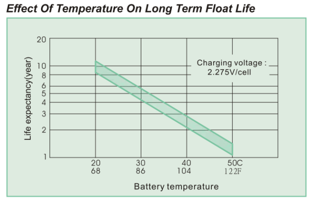
 is the expected device lifetime at the reference temperature
  .
. is the temperature increase required to halve the expected lifetime of the device.
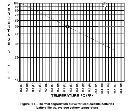


 is the peak of the signal x.


 .
.


 , where f represents the waveform. We can compute CF for either current or voltage. In this note, I focus on currents.
 )
) )
)![{{f}_{\text{rms}}}=\underset{T\to \infty }{\mathop{\lim }}\,\sqrt{\frac{1}{T}\int_{0}^{T}{{{[f(t)]}^{2}}}dt}](https://s0.wp.com/latex.php?latex=%7B%7Bf%7D_%7B%5Ctext%7Brms%7D%7D%7D%3D%5Cunderset%7BT%5Cto+%5Cinfty+%7D%7B%5Cmathop%7B%5Clim+%7D%7D%5C%2C%5Csqrt%7B%5Cfrac%7B1%7D%7BT%7D%5Cint_%7B0%7D%5E%7BT%7D%7B%7B%7B%5Bf%28t%29%5D%7D%5E%7B2%7D%7D%7Ddt%7D&bg=ffffff&fg=000&s=0&c=20201002) , where f(t) is the continuous-time parameter (usually voltage or current). The RMS value of a waveform is always greater than or equal to its average. The proof is
, where f(t) is the continuous-time parameter (usually voltage or current). The RMS value of a waveform is always greater than or equal to its average. The proof is 


.")